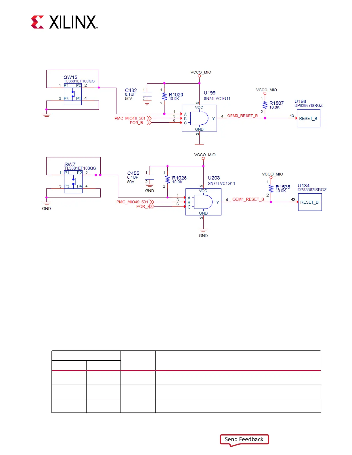
Figure 17: Ethernet PHY Reset Circuit
X24952-121420
Ethernet PHY LED Interface
[Figure 3, callout 16 and 17]
Each DP83867ISRGZ PHY (GEM0 U198, GEM1 U134) controls two LEDs in the J307 two port
connector bezel. The upper port (GEM0) yellow and green LEDs are above the port, and the
lower port (GEM1) LEDs are below the port. The PHY signal LED0 drives the green LED, and
LED1 drives the yellow LED. The LED2 signal is not used.
The LED funconal descripon is listed in the following table.
Table 16: Ethernet PHY LED Functional Description
DP83867IS PHY Pin
Type Description
Name Number
LED_2 45 S, I/O, PD By default, this pin indicates receive or transmit activity. Additional
functionality is configurable using LEDCR1[11:8] register bits.
LED_1 46 S, I/O, PD By default, this pin indicates that 100BASE-T link is established. Additional
functionality is configurable using LEDCR1[7:4] register bits.
LED_0 47 S, I/O, PD By default, this pin indicates that link is established. Additional
functionality is configurable using LEDCR1[3:0] register bits.
Chapter 3: Board Component Descriptions
UG1366 (v1.0) January 7, 2021 www.xilinx.com
VCK190 Board User Guide 43

 Loading...


