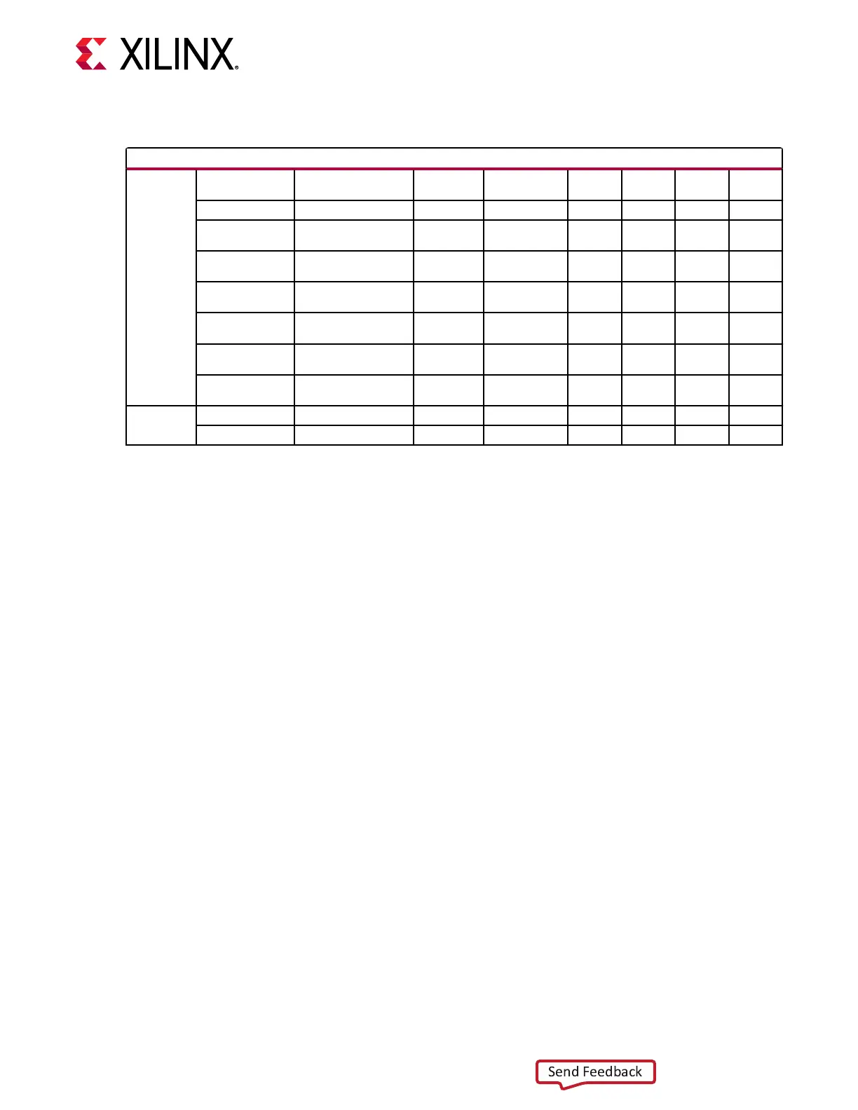
Table 23: Power System - Non-PMBus Regulators and INA226 Map (cont'd)
Non-PMBus Regulators and INA226 Map
106
8A34001_VCC_GPI
O_DC
LP38798SD-ADJ/NOPB U223 3.3 0.8 NA NA NA
8A34001_VDDA LP38798SD-ADJ/NOPB U225 3.3 0.8 NA NA NA
8A34001_VDDO_Q1
_10_7
LP38798SD-ADJ/NOPB U226 3.3 0.8 NA NA NA
8A34001_VDD_CLK
0
LP38798SD-ADJ/NOPB U227 3.3 0.8 NA NA NA
8A34001_VDDO_Q0
_9_6
LP38798SD-ADJ/NOPB U228 3.3 0.8 NA NA NA
8A34001_VDD_CLK
1
LP38798SD-ADJ/NOPB U229 3.3 0.8 NA NA NA
8A34001_VDDO_Q2
_4_11
LP38798SD-ADJ/NOPB U230 3.3 0.8 NA NA NA
8A34001_VDDO_Q8
_3_5
LP38798SD-ADJ/NOPB U236 3.3 0.8 NA NA NA
107
8A34001_VDD_FOD LP38798SD-ADJ/NOPB U231 1.8 0.8 NA NA NA
8A34001_VDDD LP38798SD-ADJ/NOPB U232 1.8 0.8 NA NA NA
More informaon about the power system regulator components can be found at the Inneon
Integrated Circuits website.
The FMCP HSPC (J51 and J53) VADJ pins are wired to the programmable rail VADJ_FMC. The
VADJ_FMC rail is programmed to 1.50V by default. The VADJ_FMC rail also powers the
XCVC1902 FMCP interface banks 706, 707, and 708 (see the table in I/O Voltage Rails).
Documentaon describing PMBus programming for the Inneon power controllers is available at
the Inneon Integrated Circuits website. The PCB layout and power system design meet the
recommended criteria described in the Versal ACAP PCB Design User Guide (UG863).
Monitoring Voltage and Current
Twenty rails have a TI INA226 PMBus power monitor circuit with connecons to the rail series
current sense resistor. This arrangement permits the INA226 to report the sensed parameters
separately on the PMBus. The rails equipped with the INA226 power monitors are shown in the
power system table in Board Power System.
As described in PMC MIO[46:47] I2C0 Bus, the I2C0 bus provides access to the PMBus power
controllers and the INA226 power monitors via the U33 TCA9548A bus switch. All PMBus
controlled Inneon regulators are ed to the PMBUS_SDA/SCL PMBus, while the INA226 power
monitors are split across PMBUS1_INA226_SDA/SCL and PMBUS2_INA226_SDA/SCL.
The I2C0 bus topology gure and I2C0 port expander TCA6416A U233 address 0x20
connecons table in PMC MIO[46:47] I2C0 Bus document the I2C0 bus access path to the
Inneon PMBus controllers and INA226 power monitor op amps. Also, see schemac
038-05005-01. These power system components are also accessible to the ZU4 U125 system
controller (bank 501) and the ACAP U1 (bank 501).
Chapter 3: Board Component Descriptions
UG1366 (v1.0) January 7, 2021 www.xilinx.com
VCK190 Board User Guide 68

 Loading...


