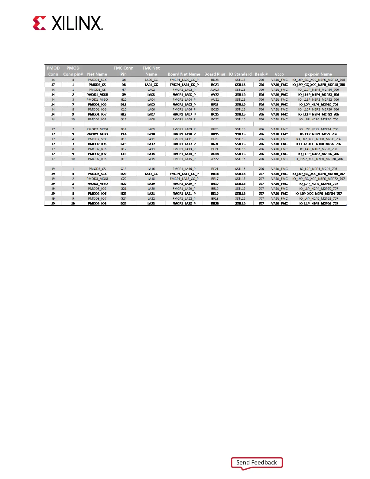
Figure 30: Pmod FMC Pin Mapping
X24767-102620
This pin mapping can translate between the VCK190 and VMK180 boards. There is no dierence
in pin mapping. The signal voltage is controlled by the VADJ, which is set by the system
controller. The default is 1.5V for VADJ and this should never be changed. This must match the
I/O standard voltage, otherwise it is possible to cause damage to the I/O. The I/O standard used
is typically SSTL15 (see Figure 29), but any 1.5V standard can be used for Pmod compliance. The
TXS0108E level translator has a minimum signal voltage of 1.4V, which means only 1.5V I/O
standards can be used with this PMOD FMC board.
Appendix C: Pmod FMC
UG1366 (v1.0) January 7, 2021 www.xilinx.com
VCK190 Board User Guide 73

 Loading...


