GTY105: HSDP and 2x zSFP
GTY105 channel 1 is not used.
The GTY105 channel 0 high-speed debug port is a new feature that will be supported in the
future. GTY105 REFCLK1 receives the HSDP_SI570_CLK from Si570 U5 (default frequency
156.25 MHz).
GTY105 channel 2 is wired to SFP0 and channel 3 is wired to SFP1. The two zSFPs are
implemented in a dual-port stacked connector J287 (SFP0 lower, SFP1 upper). Each SFP has an
I2C connecon to the I2C1 bus through the I2C mulplexer (TCA9548PWR U214) as
documented in PMC MIO[44:45] I2C1 Bus.
GTY105 REFCLK0 receives the zSFP_SI570_CLK from Si570 U192 (default frequency 156.25
MHz).
zSFP/zSFP+ Module Connector
[Figure 3, callout 13]
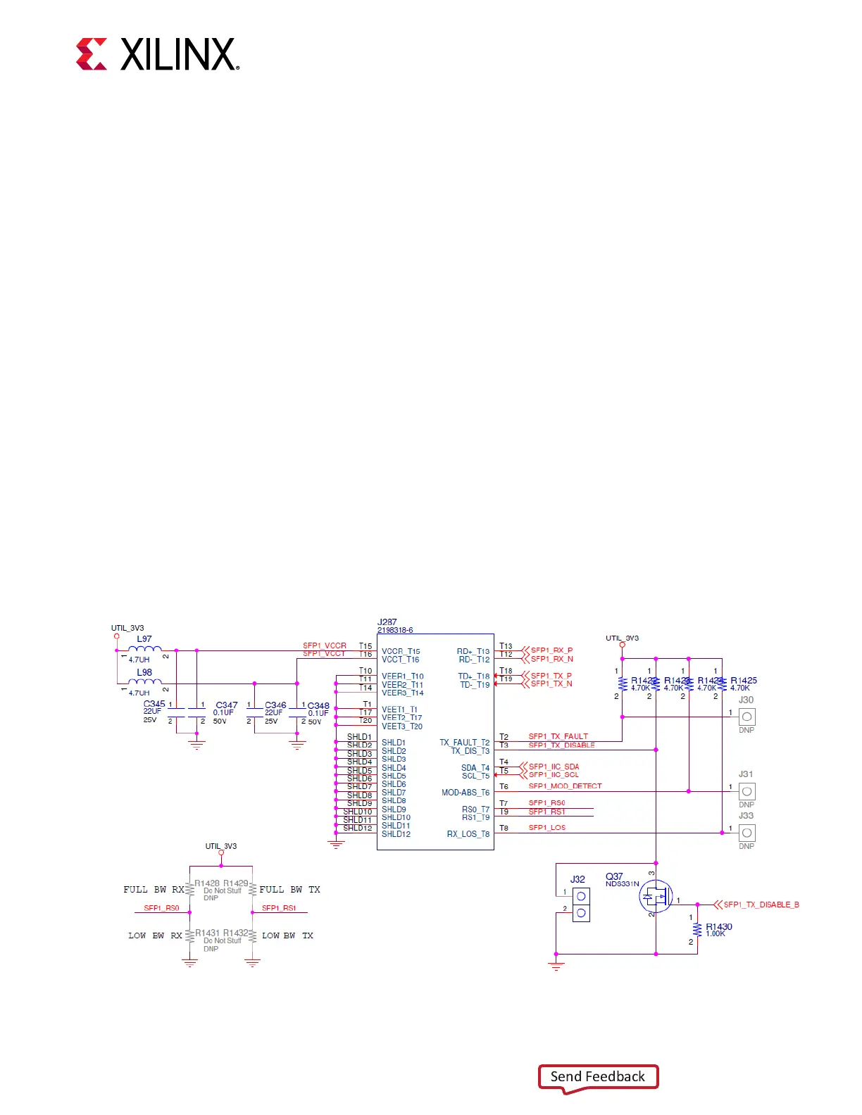
The VCK190 board hosts dual-port zSFP/zSFP+ J287, which accepts zSFP or zSFP+ modules.
The following gure shows the zSFP/zSFP+ module connector circuitry typical of the two
implementaons.
Figure 20: zSFP/zSFP+ Module Connector
X24953-121420
Chapter 3: Board Component Descriptions
UG1366 (v1.0) January 7, 2021 www.xilinx.com
VCK190 Board User Guide 53

 Loading...


