○ Q1: SI570_8A34001_MUX_BUF1_P/N capacitor coupled to GTY204
FMCP2_DP[0:3]_C2M/M2C interface GTY_REFCLK0 pins G13 (P) and G12 (N)
○ Q2: SI570_8A34001_MUX_BUF2_P/N capacitor coupled to GTY205
FMCP2_DP[4:7]_C2M/M2C interface GTY_REFCLK0 pins E13 (P) and E12 (N)
○ Q3: SI570_8A34001_MUX_BUF3_P/N capacitor coupled to GTY206
FMCP2_DP[8:11]_C2M/M2C interface GTY_REFCLK0 pins C13 (P) and C12 (N)
The connecon details for ACAP U1 connected clocks described in this secon are documented
in the VCK190 board XDC le, referenced in Appendix B: Xilinx Design Constraints.
For more details on the Silicon Labs SI570, SI5332, and SI53340 devices, see the Silicon Labs
website.
For more details on the IDT 85411AMLF, 8T49N241, and 8A34001 devices, see the Integrated
Device Technology, Inc. website.
For Versal ACAP clocking informaon, see the Versal ACAP Clocking Resources Architecture Manual
(AM003).
IEEE-1588 eCPRI Programmable Synchronization Management Unit
[Figure 3, callout 46]
GTY Transceivers
[Figure 3, callout 1]
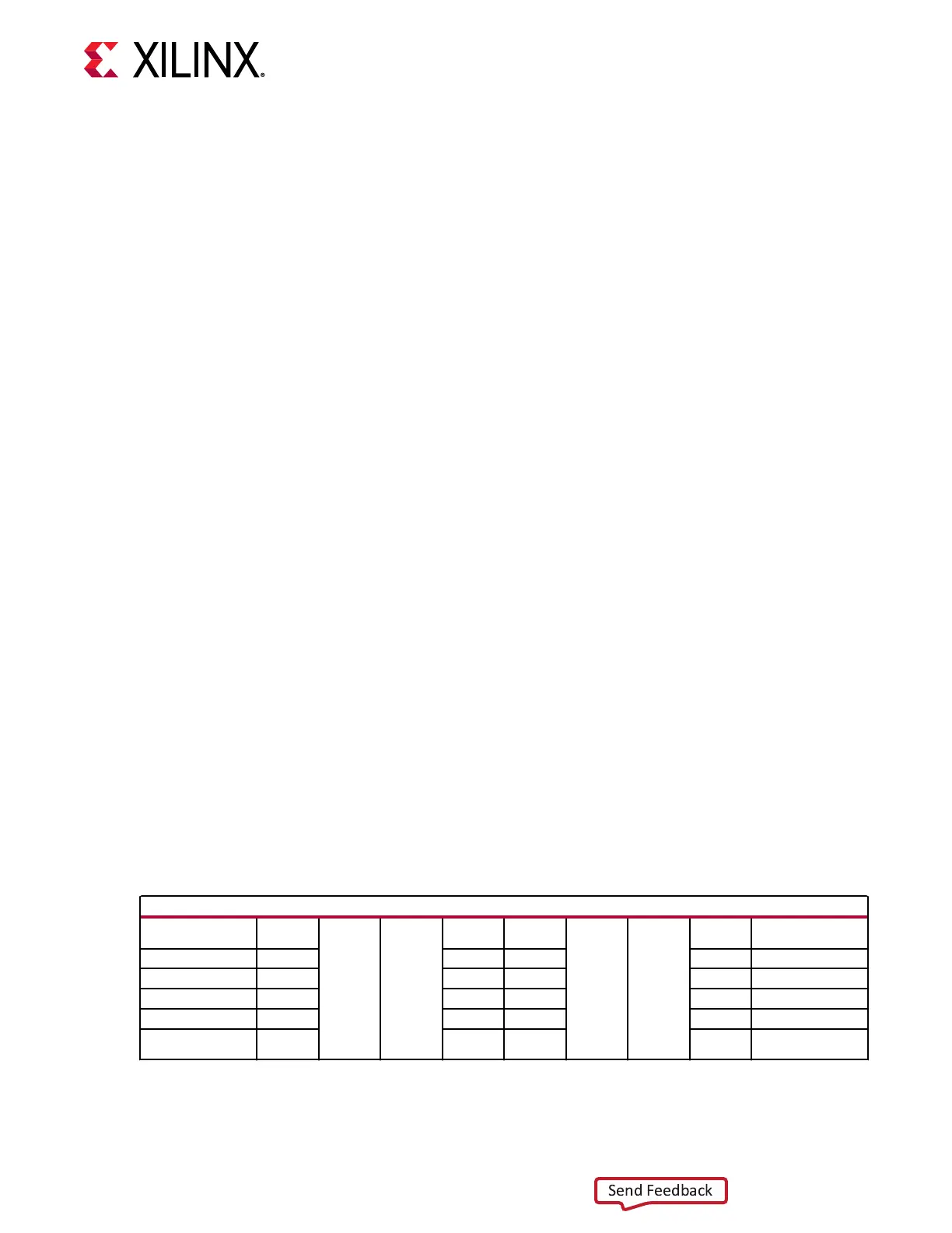
The GTY transceivers in the XCVC1902 ACAP U1 are grouped into four channels or quads. The
XCVC1902 has four GTY quads (GTYs 103-106) on the right side of the device and seven GTY
quads (GTYs 200-206) on the le side of the device.
The VCK190 board provides access to 11 of the 11 GTY quads as shown in the GTY map in the
following table.
Table 18: GTY Mapping
VCK190 XC10S80 VSVA2197 GTY Mapping
HDMI_TX_CLK_LVDS (TX
only)
ch3
GTYT_S
Quad 106
GTYT_S
Quad 206
ch3 FMC2 DP11
HDMI Lane 2 ch2 ch2 FMC2 DP10
HDMI Lane 1 ch1 ch1 FMC2 DP9
HDMI Lane 0 ch0 ch0 FMC2 DP8
HDMI_9T49N241_CLK refclk1 refclk1 FMC2_GBTCLK2
HDMI_RX_CLK refclk0 refclk0
SI570_8A34001_MUX_BU
F3
Chapter 3: Board Component Descriptions
UG1366 (v1.0) January 7, 2021 www.xilinx.com
VCK190 Board User Guide 50

 Loading...


