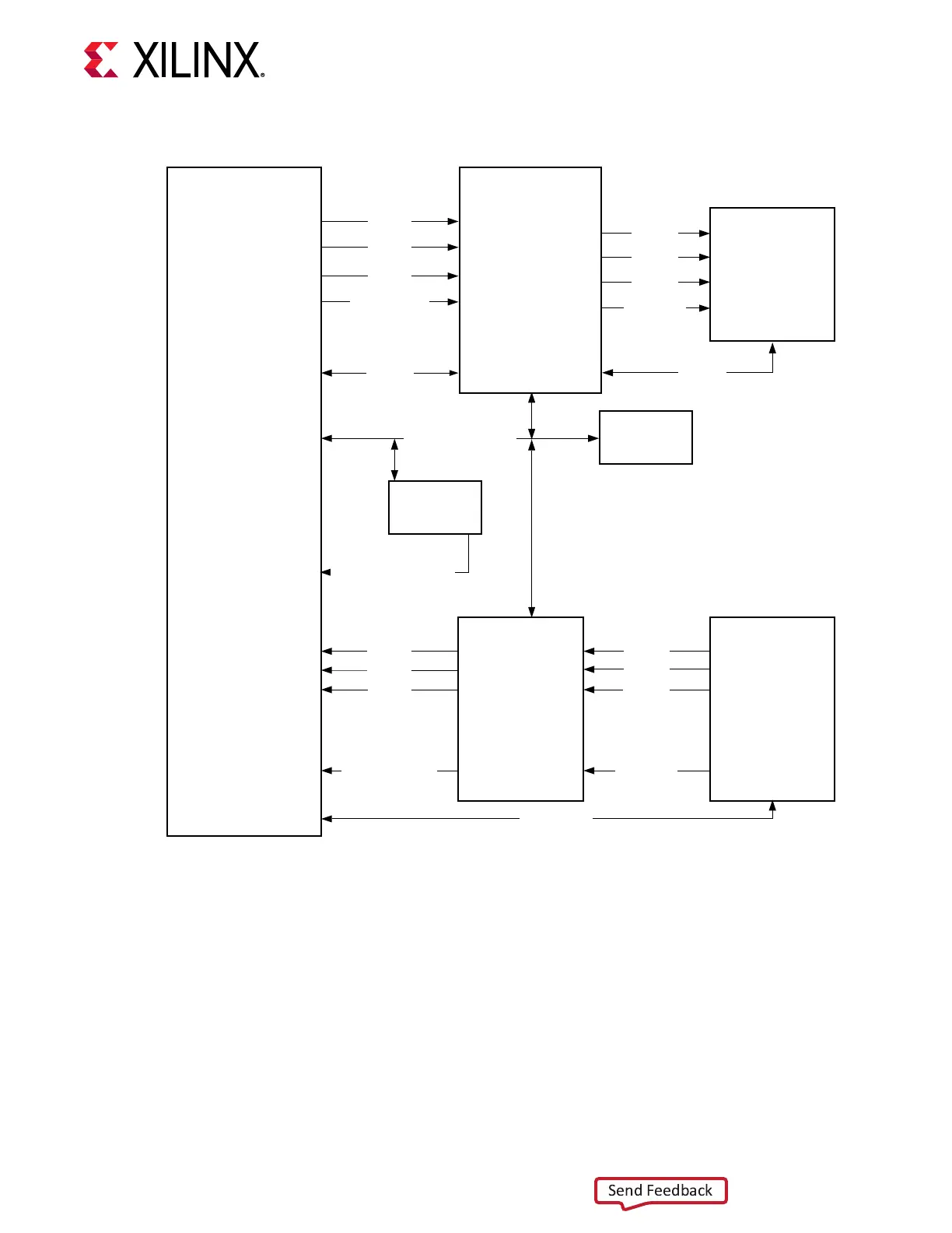
Figure 22: HDMI Interface Block Diagram
HDMI
IP
HDMI_0
DRIVER
(SN65DP159)
HDMI_1
HDMI_2
TX_CLK_LVDS
I2C_SRC
I2C_CTL_HDMI_OUT
8T49N241
EDID
EEPROM
TMDS181 and
Termination
Network
HDMI_IN
HDMI_OUT
TMDS_0
TMDS_1
TMDS_2
TMDS_CLK
I2C_SNK
HDMI_8T49N241_OUT
HDMI_0
HDMI_1
HDMI_2
RX_GTH_REFCLK
TMDS_0
TMDS_1
TMDS_2
TMDS_CLK
I2C_HDMI_IN
X23206-091019
The VCK190 board accepts HDMI video input on the TE Connecvity 1888811-1 right-angle
dual-stacked HDMI type-A receptacle P2 (lower port). The HDMI TMDS signals are input to TI
TMDS181 remer U55, which then drives the series capacitor coupled HDMI RX signals to U1
XCVC1902 GTY bank 106. The VCK190 HDMI RX interface supports up to 4K 60 Hz
resoluons. See the Xilinx HDMI IP documentaon for more details about resoluons, color
spaces, and oponal HDCP features supported by the U1 Versal ACAP.
The HDMI clock recovery is detailed in PCIe Clock.
For Xilinx HDMI IP details, see the HDMI 1.4/2.0 Transmier Subsystem Product Guide (PG235)
and the HDMI Transmier and Receiver Subsystem Answer Record 70514.
Chapter 3: Board Component Descriptions
UG1366 (v1.0) January 7, 2021 www.xilinx.com
VCK190 Board User Guide 57

 Loading...


