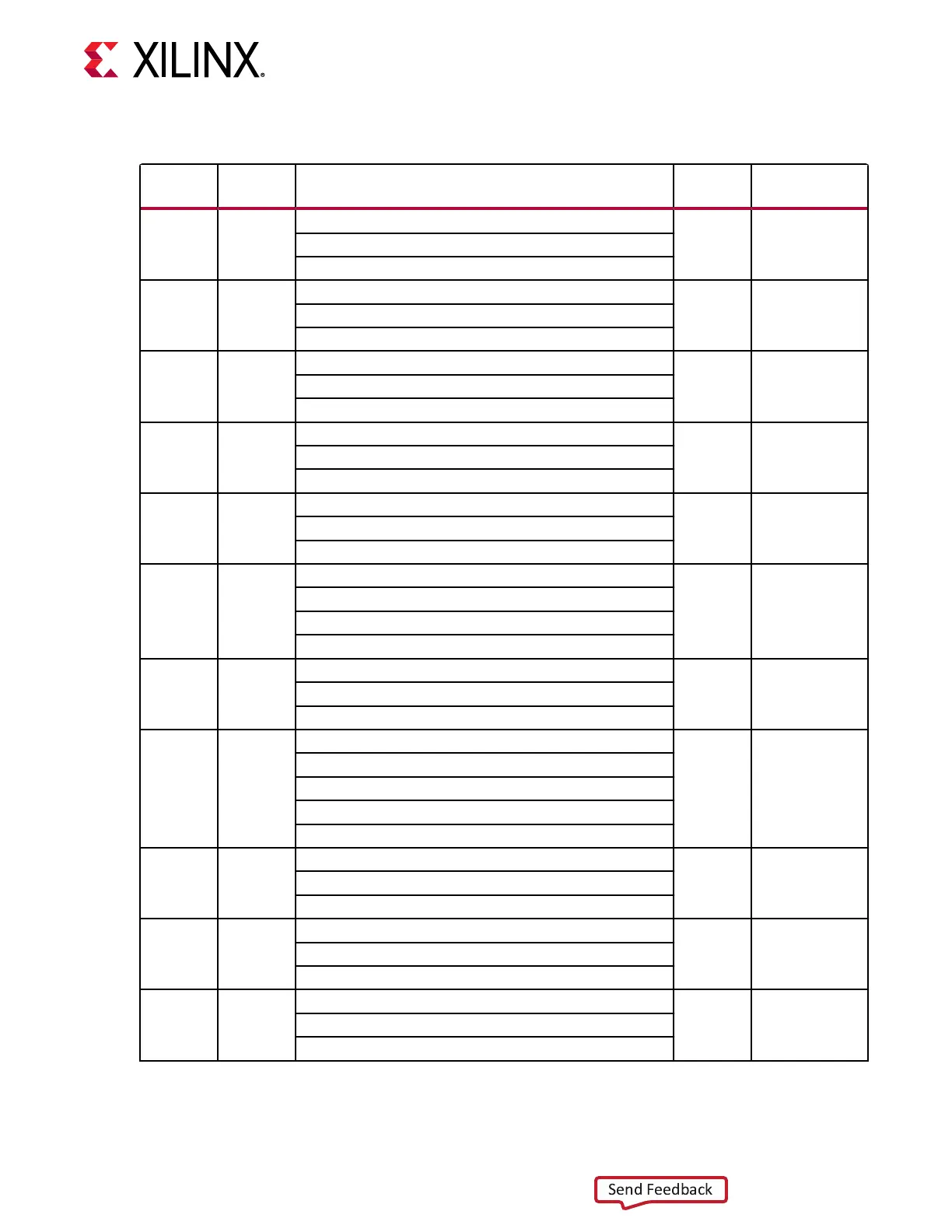
Table 3: Default Jumper Settings (cont'd)
Callout
Number
Ref. Des. Function Default
Schematic
Page
2 J26
POR_B sense select
1-2 15
1-2: VCCO_503
2-3: VCCAUX_PMC
3 J32
SFP1_TX_DISABLE select
ON 45
ON: enable always
OFF: disable/allows ACAP U1 control
4 J34
ACAP U1 bank VCC_FUSE select
2-3 17
1-2: VCC1V8
2-3: GND
5 J35
SFP0_TX_DISABLE select
ON 17ON: enable always
OFF: disable/allows ACAP U1 control
6 J37
JTAG MUX U14/U15 OE_B
2-3 24
1-2: UTIL_3V3 disable
2-3: GND enable
7 J60
PCIe lane size select
5-6 46
1-2: x1
3-4: x4
5-6: x8
8 J203
SYSCTLR_POR_B enable
ON 89ON: enable
OFF: disable
9 J205
System Controller M88E1512 EPHY U131 configuration
7-8 95
1:2: GND (5'b00000)
3:4: SYSCTLR_ETH_LED0
5:6: SYSCTLR_ETH_LED0
7:8: SYS_VCC1V8 (5'b00001)
10 J234
ACAP cooling fan control
2-3 54
1-2: MAX6643 U64 control is enabled
2-3: always on
8 J300
ULPI USB3320 U99 USB conn. J308 shield select
1-2 421-2: J308 shield directly to GND
2-3: J308 shield capacitor C2762 to GND
8 J301
IP4856 U104 VERSAL_SD1_REF voltage select
1-2 761-2: UTIL_3V3
2-3: GND
Chapter 2: Board Setup and Configuration
UG1366 (v1.0) January 7, 2021 www.xilinx.com
VCK190 Board User Guide 19

 Loading...


