The USB3320 is clocked by a 24 MHz crystal (X8). See the Standard Microsystems Corporaon
(SMSC) USB3320 data sheet for clocking mode details. The interface to the USB3320 PHY is
implemented through the IP in the XCVC1902 ACAP PS.
The USB3320 ULPI transceiver circuit has a Micrel MIC2544 high-side programmable current
limit switch (U100). This switch has an open-drain output fault ag on pin 2, which turns on red
LED DS37 if over current or thermal shutdown condions are detected. DS37 is located just
above the U125 system controller component (callout 48 in the gure in Board Component
Locaon).
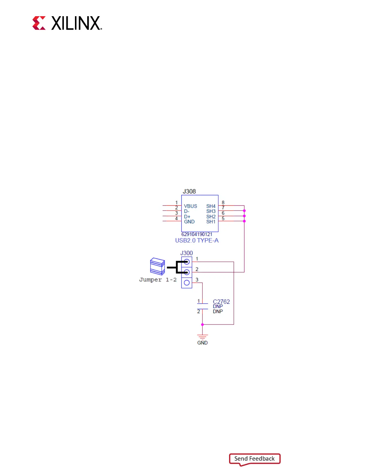
Note: As shown in the following gure, the shield for the USB 2.0 type-A connector (J308) can be ed to
GND by a jumper on header J300 pins 1-2 (default). The USB shield can oponally be connected through a
series capacitor to GND by installing a capacitor (body size 0402) at locaon C2762 and jumping pins 2-3
on header J300.
Figure 10: USB3320 USB2.0 Connector J308 Shield Connection Options
X24950-121420
The detailed ACAP connecons for the feature described in this secon are documented in the
VCK190 board XDC le, referenced in Appendix B: Xilinx Design Constraints.
PMC MIO[26:36, 51] Bank 501: Secure Digital (SD)
Card IF (J302)
[Figure 3, callout 10]
Chapter 3: Board Component Descriptions
UG1366 (v1.0) January 7, 2021 www.xilinx.com
VCK190 Board User Guide 31

 Loading...


