ZC702 Board User Guide www.xilinx.com 15
UG850 (v1.7) March 27, 2019
Feature Descriptions
The PS integrates two Arm® Cortex™-A9 MPCore™ application processors, AMBA®
interconnect, internal memories, external memory interfaces, and peripherals including
USB, Ethernet, SPI, SD/SDIO, I2C, CAN, UART, and GPIO. The PS runs independently of the PL
and boots at power-up or reset.
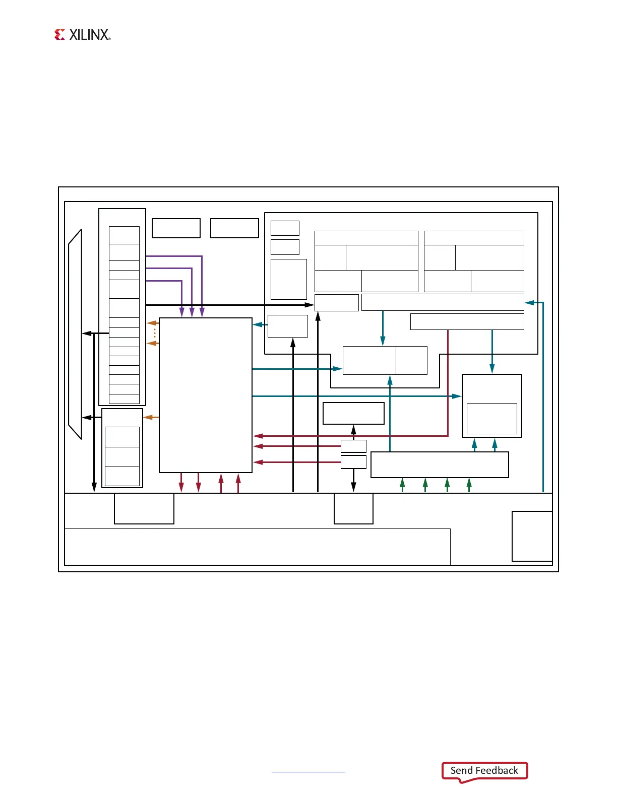
A system level block diagram is shown in Figure 1-4.
For additional information on Zynq-7000 SoC devices, see the Zynq-7000 SoC Data Sheet:
Overview (DS190) [Ref 1]
, and the Zynq-7000 SoC Technical Reference Manual (UG585)
[Ref 2] for more information about Zynq-7000 SoC configuration options.
X-Ref Target - Figure 1-4
Figure 1-4: Zynq-7000 SoC Block Diagram
2x USB
2x GigE
2x SD
Zynq-7000 SoC
I/O
Peripherals
IRQ
IRQ
EMIO
SelectIO
Resources
DMA 8
Channel
CoreSight
Components
Programmable Logic
DAP
DevC
SWDT
DMA
Sync
Notes:
1) Arrow direction shows control (master to slave)
2) Data flows in both directions: AXI 32-Bit/64-Bit, AXI 64-Bit, AXI 32-Bit, AHB 32-Bit, APB 32-Bit, Custom
ACP
256K
SRAM
Application Processor Unit
TTC
System-
Level
Control
Regs
GigE
CAN
SD
SDIO
UART
GPIO
UART
CAN
I2C
SRAM/
NOR
ONFI 1.0
NAND
Processing System
Memory
Interfaces
Q-SPI
CTRL
USB
GigE
I2C
USB
SD
SDIO
SPI
SPI
Programmable Logic to
Memory Interconnect
MMU
FPU and NEON Engine
Snoop Controller, AWDT, Timer
GIC
32 KB
I-Cache
ARM Cortex-A9
CPU
ARM Cortex-A9
CPU
MMU
FPU and NEON Engine
Config
AES/
SHA
XADC
12-Bit ADC
Memory
Interfaces
512 KB L2 Cache and Controller
OCM
Interconnect
DDR2/3,
LPDDR2
Controller
UG850_c1_04_062918
32 KB
D-Cache
32 KB
I-Cache
32 KB
D-Cache
MIO
Clock
Generation
Reset
Central
Interconnect
General-Purpose
Ports
High-Performance Ports