ZC702 Board User Guide www.xilinx.com 24
UG850 (v1.7) March 27, 2019
Feature Descriptions
The connections between the USB 2.0 PHY at U9 and the XC7Z020 SoC are listed in
Table 1-8.
Figure 1-7 shows the USB 2.0 ULPI Transceiver circuitry. Note that the shield for the USB
Mini-B connector (J1) can be tied to GND by a jumper on header J36 pins 1–2 (default). The
USB shield can optionally be connected through a capacitor to GND by installing a
capacitor (body size 0402) at location C202 and jumping pins 2-3 on header J36.
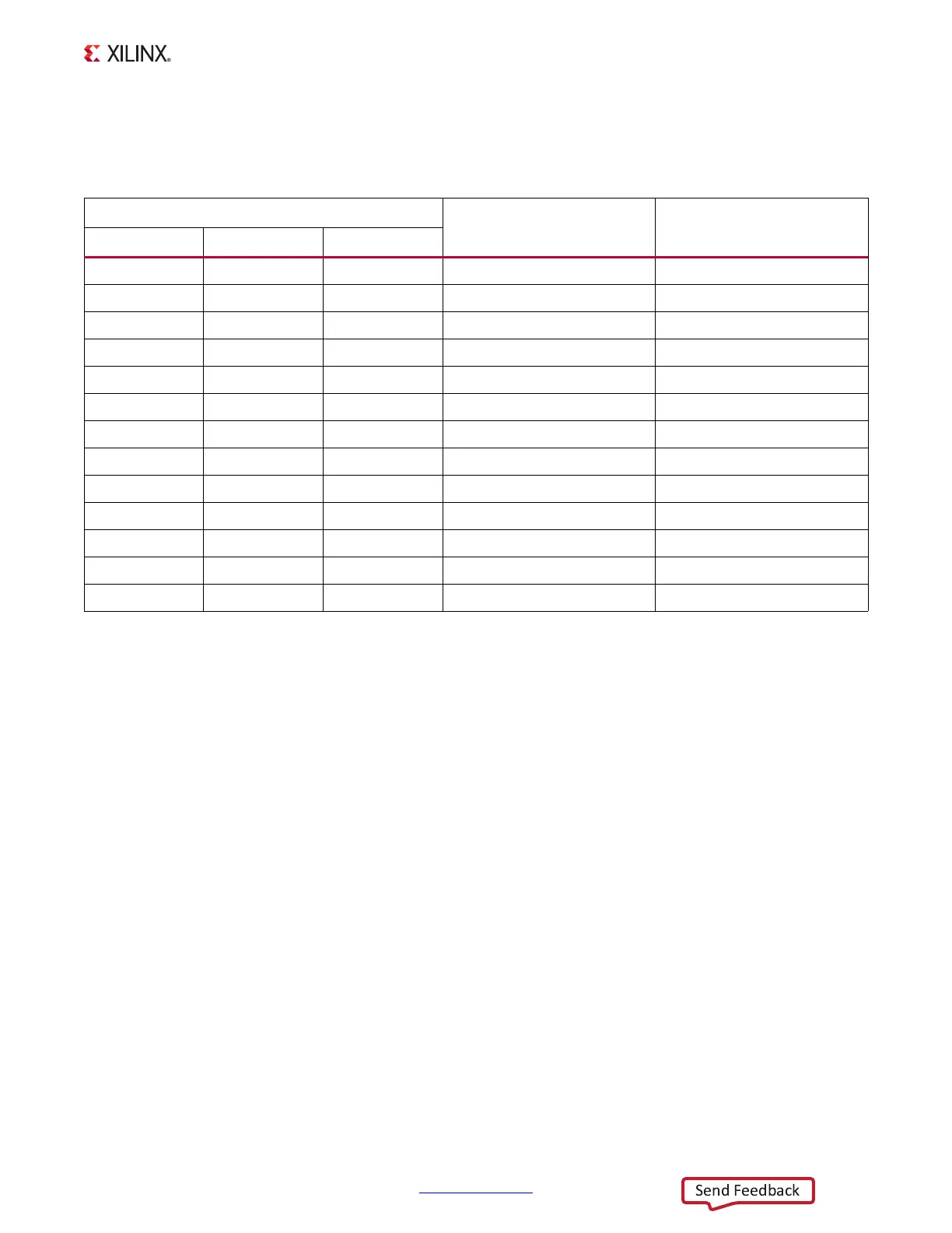
Table 1-8: USB 2.0 ULPI Transceiver Connections to the XC7Z020 SoC
XC7Z020 (U1)
Schematic Net Name USB3320 (U9) Pin
Pin Name Bank Pin Number
PS_MIO36 501 A9 USB_CLKOUT 1
PS_MIO31 501 F9 USB_NXT 2
PS_MIO32 501 C7 USB_DATA0 3
PS_MIO33 501 G13 USB_DATA1 4
PS_MIO34 501 B12 USB_DATA2 5
PS_MIO35 501 F14 USB_DATA3 6
PS_MIO28 501 A12 USB_DATA4 7
PS_MIO37 501 B14 USB_DATA5 9
PS_MIO38 501 F13 USB_DATA6 10
PS_MIO39 501 C13 USB_DATA7 13
PS_MIO30 501 A11 USB_STP 29
PS_MIO29 501 E8 USB_DIR 31
PS_MIO7 500 D5 USB_RESET_B_AND 27 (through AND gate U62)