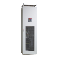
Manual Power Quality Filter PQFM Hardware description 29
Table 12: PQF main controller board description
Item Description
diagram
designation
System connector: 24 V power supply to control board
bus connection from previous filter unit
CAN bus connection to next filter unit
System connector: Power supply and CAN communication to PQF Manager
System connector: 230 V power supply to control board
em connector: Main contactor control
System connector
System connector: Coming from CT terminal X21 (internal)
System connector: Supply and DC link voltage measurement
15-16
System connector: control of IGBT
with ABB logo at bottom left
LED 3: ON: Critical error in filter unit considered (red LED)
LED 3: OFF: No critical error in filter unit considered
LED 2: ON: PQF unit running or in startup process (Armed)
LED 2: OFF: PQF unit off and not in startup process
LED 1: Blinking at regular interval (1 s): Microcontroller running properly
LED 1: ON, OFF or blinking irregularly: Microcontroller not running properly
with ABB logo at bottom left
LED 5: ON: Filter unit is acting as the master of the complete system
LED 5: OFF: Filter unit is acting as a slave in the filter system
LED 4: Blinking at regular interval (1 s): DSP processor running properly
LED 4: ON, OFF or blinking irregularly: DSP processor not running properly
Filter unit address selector (3
left) and CAN bus termination (top DIP switch):
Symbols used: R: right – L: left
Address 1: Position of the 3 switches starting from bottom: RRR
Address 2: Position of the 3 switches starting from bottom: LRR
Address 3: Position of the 3 switches starting from bottom: RLR
Address 4: Position of the 3 switches starting from bottom: LLR
Address 5: Position of the 3 switches starting from bottom: RRL
Address 6: Position of the 3 switches starting from bottom: LRL
Address 7: Position of the 3 switches starting from bottom: RLL
Address 8: Position of the 3 switches starting from bottom: LLL
Note: In a multi-master arrangement, the master which is operational and
which has the lowest address controls the system.
The default address setting is RRR
CAN bus termination (top DIP switch):