Figure 98. The Sequence of Bulk Erase of Flash Memory ................................................................. 178
Figure 99. ISP Mode ........................................................................................................................... 182
Figure 100. Configuration of the Extended Stack Pointer ................................................................... 190
Figure 101. OCD 1 and OCD 2 Connector Pin Diagram .................................................................... 192
Figure 102. Debugger (OCD1/OCD2) and Pinouts ............................................................................ 193
Figure 103. On-Chip Debugging System in Block Diagram ................................................................ 194
Figure 104. Timing Diagram of Debug Mode Entry ............................................................................ 194
Figure 105. 10-bit Transmission Packet .............................................................................................. 196
Figure 106. Data Transfer on OCD ..................................................................................................... 196
Figure 107. Bit Transfer on Serial Bus ................................................................................................ 197
Figure 108. Start and Stop Condition .................................................................................................. 197
Figure 109. Acknowledge on Serial Bus ............................................................................................. 198
Figure 110. Clock Synchronization during Wait Procedure ................................................................. 198
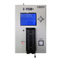
Figure 111. E-PGM+ (Single Writer) and Pinouts ............................................................................... 199
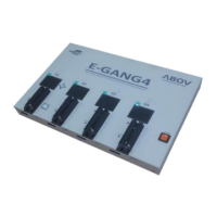
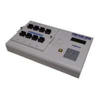
Figure 112. E-Gang4 and E-Gang6 (for Mass Production) ................................................................. 200
Figure 113. Connection of Transmission ............................................................................................. 201
Figure 114. PCB Design Guide for On-Board Programming .............................................................. 203


 To Next Page