10 Installation
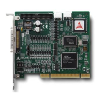
2.2 PCI-8102 Outline Drawing
Figure 2-1: PCB Layout of the PCI-8102
P1: Input / Output Signal Connector (68-pin)
P2: 16 Digital Input / Output Signals Connector
K1 / K2: Simultaneous Start / Stop Connector
SW1: DIP switch for card index selection (0-15)
J8-J11: Pulse output selection jumper
119.91
121.7 5
106.68
100 .33
126 .35
 Loading...