Signal Connections 21
The following wiring diagram is for OUT and DIR signals on the 2
axes.
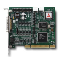
PCI-8102:
NOTE: If the pulse output is set to open collector output mode,
OUT- and DIR- are used to transmit OUT signals. The sink current
must not exceed 20mA on the OUT- and DIR- pins. The default
setting of jumper is 1-2 shorted. The default setting is 1-2 shorted.
Suggest Usage: Jumper 2-3 shorted and connect OUT+/DIR+ to a
470 ohm pulse input interface’s COM of driver. See the following
figure.
Warning: The sink current must not exceed 20mA or the 26LS31
will be damaged!
VDD
VCC
4.7
OUT/DIR
26LS31
J8-J11
OUT+/DIR+
OUT-/DIR-
EXGND
1
2
3
VDD
OUT+, DIR+
OUT-, DIR-
EXGND
470 Ohm
+5V
Inside Motion Card
Inside Motor Driver
 Loading...