ADV7511W HARDWARE USER’S GUIDE
Rev.A
Page 14
of 45
Rev A
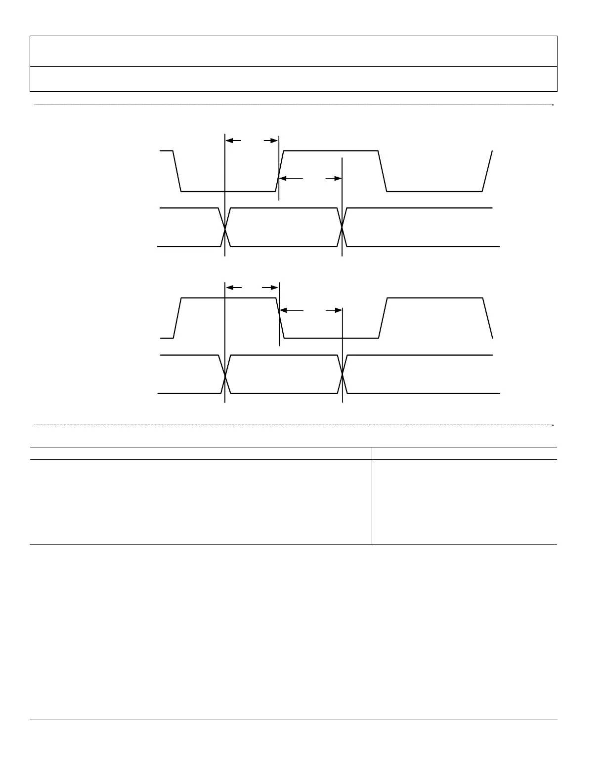
Figure 4
Timing for S/PDIF Audio Interface
Table 2 Absolute Maximum Ratings
Parameter Rating
Digital Inputs (SDA, SCL, DDCSDA, DDCSCL, HPD, PD, CEC) −0.3 V to +5.5 V
Audio/Video Digital Inputs (MCLK, SPDIF, I2S[3:0], SCLK, HSYNC, DE, VSYNC, CEC_CLK) −0.3 V to +3.63 V
Digital Output Current 20 mA
Operating Temperature Range -40°C to +105°C
Storage Temperature Range -65°C to +150°C
Maximum Junction Temperature 150°C
Maximum Case Temperature 150°C
Stresses above those listed under Absolute Maximum Ratings may cause permanent damage to the device. This is a stress rating
only; functional operation of the device at these or any other conditions above those indicated in the operational section of this
specification is not implied. Exposure to absolute maximum rating conditions for extended periods may affect device reliability.
Voltage ratings assume that all power supplies are at nominal levels.
t
ASU
Audio data:
S/PDIF
MCLK
Rising Edge
t
AHLD
Valid data
R0x0B[6] = 0
t
ASU
MCLK
Falling Edge
Valid data
R0x0B[6] = 1
t
AHLD
Audio data:
S/PDIF
 Loading...