ADV7511W HARDWARE USER’S GUIDE
Rev.A
Page 42
of 45
Rev A
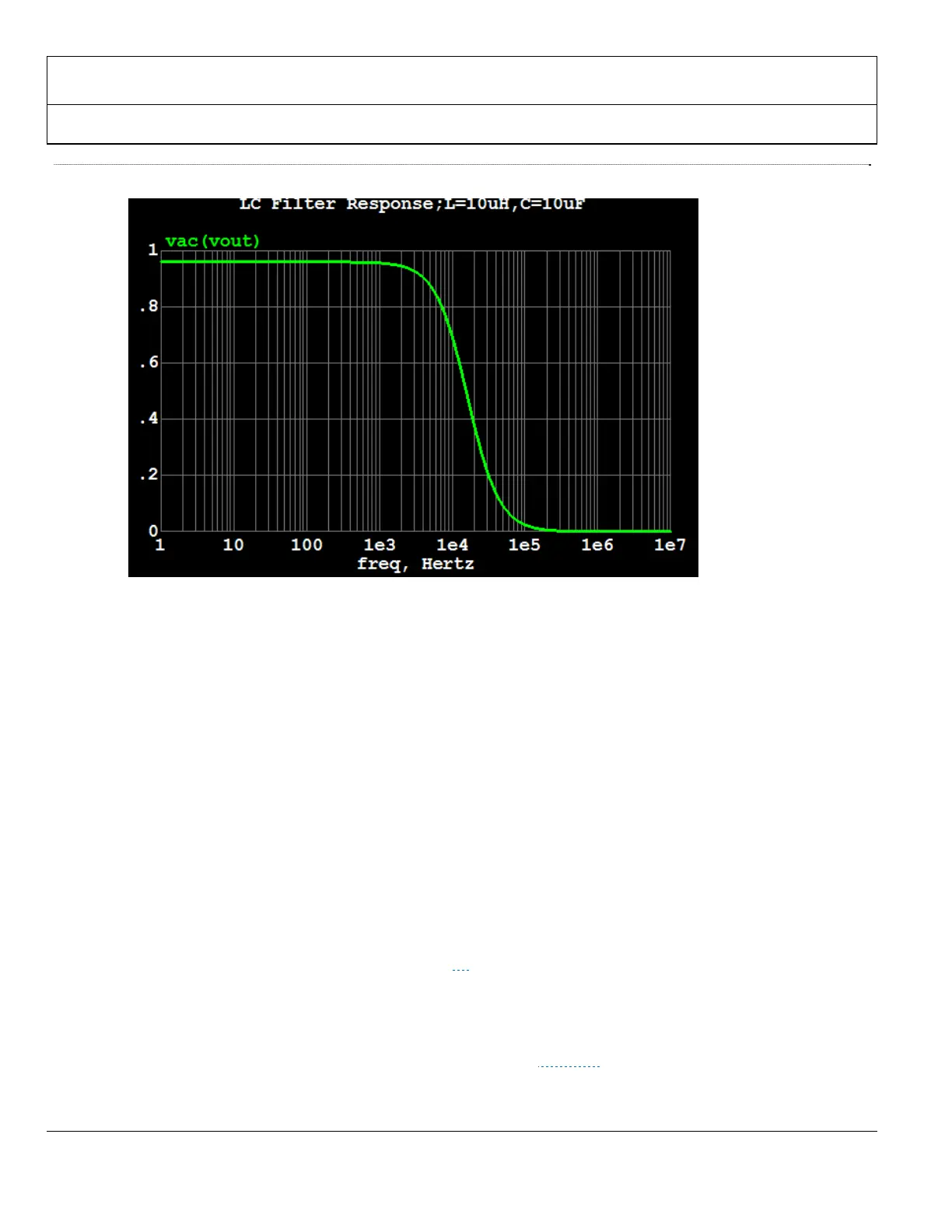
Figure 23
LC Filter Transfer Curve
7.2
Video Clock and Data Inputs
Any noise that that is coupled onto the CLK input trace will add jitter to the system. It is a recommended to control the
impedance of the CLK trace. If possible, using a solid ground or supply reference under the trace is a good way to
ensure the impedance remains constant over the entire length of the trace. Therefore, minimize the video input data
clock (pin 53) trace length and do not run any digital or other high frequency traces near it. Make sure to match the
length of the input data signals to optimize data capture especially for Double Data Rate (DDR) input formats.
7.3
Audio Clock and Data Inputs
The length of the input audio data signals should be matched as closely as possible to optimize audio data capture. It is
recommended to add series 50Ω resistors (+/-5%) as close as possible to the source of the audio data and clock signals
to minimize impedance mismatch.
7.4
SDA and SCL
The SDA and SCL pins should be connected to an I2C Master. A pull-up resistor of 2kΩ (+/-10%) to 1.8V or 3.3V is
recommended for each of these signals. See ▶ Figure 25
.
7.5
DDCSDA and DDCSCL
The DDCSDA and DDCSCL pins should be connected to the HDMI connector. A pull-up resistor of 1.5 kΩ to 2kΩ
(+/-10%) to HDMI +5V is required for each of these signals. See ▶
Figure 25.
 Loading...