ADV7511W HARDWARE USER’S GUIDE
Rev. A
Page 39
of 45
Rev A
■
Stop signal
Figure 20
Serial Interface—Typical Byte Transfer
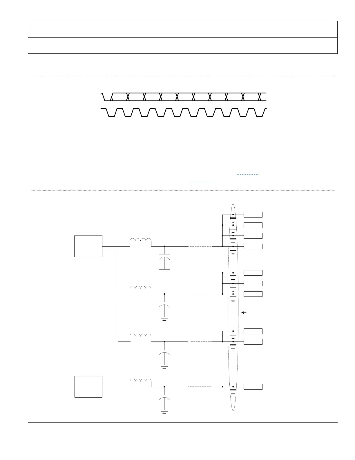
6.7
Power Domains
All power domains of the ADV7511W operate off of 1.8 volts, with the exception of the DVDD_3V which is 3.3 volts.
It is recommended that the ADV7511W has its own designated 1.8V linear regulator and that the PVDD, AVDD and
DVDD PCB power domains be segregated using inductors as illustrated in ▶ Figure 21
. More detailed
recommendations for the PCB can be found in section ▶ Section 7:.
Figure 21
Power Supply Domains
BIT 7
ACKBIT 6 BIT 5 BIT 4 BIT 3 BIT 2 BIT 1 BIT 0SDA
SCL
05087-008
1.8V
LDO
10uF
10uH
10uF
10uH
DVDD
AVDD
10uF
10uH
PVDD
Pin 51
DVDD
Pin 31
DVDD
Pin 11
DVDD
Pin 1
DVDD
Pin 19
AVDD
Pin 15
AVDD
PVDD
Pin 12
BGVDD
All bypass capacitors 0.1uF
3.3V
LDO
10uF
10uH
Pin 29
DVDD_3V
Pin 25
AVDD
Pin 13
 Loading...