ADV7511W HARDWARE USER’S GUIDE
Rev. A
Page 11
of 45
Rev A
SECTION 4: SPECIFICATIONS
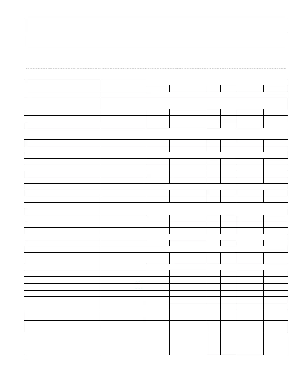
Table 1 Electrical Specifications
Parameter Conditions
ADV7511W
Temp Test Level
1
Min Typ Max Unit
DIGITAL INPUTS
Data Inputs – Video, Audio and
CEC_CLK
Input Voltage, High (V
IH
) Full VI 1.35 3.5 V
Input Voltage, Low (V
IL
) Full VI -0.3 0.7 V
Input Capacitance 25°C VIII 1.0 1.5 pF
I2C Lines (DDCSDA, DDCSCL, SDA,
SCL)
Input Voltage, High (V
IH
) Full VI 1.19 5.5 V
Input Voltage, Low (V
IL
) Full VI -0.3 0.8 V
CEC
Input Voltage, High (V
IH
) Full VI 2.0 5.5 V
Input Voltage, Low (V
IL
) Full VI -0.3 0.8 V
Output Voltage, High (V
IH
) Full VI 2.5 3.63 V
Output Voltage, Low (V
IL
) Full VI -0.3 0.6 V
HPD
Input Voltage, High (V
IH
) Full VI 1.3 5.5 V
Input Voltage, Low (V
IL
) Full VI -0.3 0.8 V
THERMAL CHARACTERISTICS
Thermal Resistance
θ
JC
Junction-to-Case Full V 20 °C/W
θ
JA
Junction-to-Ambient Full V 43 °C/W
Ambient Temperature Full V -40 +25 +105 °C
DC SPECIFICATIONS
Input Leakage Current, I
IL
25°C VI −1 +1 μA
POWER SUPPLY
1.8V Supply Voltage (DVdd, AVdd,
PVdd, BGVdd)
Full IV 1.71 1.8 1.90 V
1.8V Supply Voltage Noise Limit
DVdd – HDMI Digital Core Full V
64
mV RMS
AVdd – HDMI Analog Core
Refer to ▶Section 7.1
Full V mV RMS
PLVdd – HDMI PLL – Analog
Refer to ▶Section 7.1
Full V mV RMS
PVdd – HDMI PLL - Digital Full V
64
mV RMS
BGVdd - Band-gap Full V
64
mV RMS
3.3V Supply Voltage (DVdd_3V) Full 3.15 3.3 3.45 V
Power-Down Current – level 1
Refer to the ADV7511
Programming Guide
25°C IV 20 mA
Power-Down Current – level 2
Refer to the ADV7511
Programming Guide
25°C IV 300 μA
Transmitter Total Power
1.8V power = 325mW
3.3V power = 1mW
1080p, 24 bit, typical
random pattern
Full VI 326 mW
 Loading...