ADV7511W HARDWARE USER’S GUIDE
Rev. A
Page 23
of 45
Rev A
Table 7
YCbCr 4:2:2 Formats (12, 10, or 8 bits) Input Data Mapping:
0x48[4:3]=‘00’ (evenly distributed) Input ID = 3,4,7,8
Input
Format
Data <23:0>
23 22 21 20 19 18 17 16 15 14 13 12 11 10 9 8 7 6 5 4 3 2 1 0
Style 1
12 bit Cb/Y/Cr/Y[11:4] [3:0]
10 bit Cb/Y/Cr/Y[9:2] [1:0]
8 bit Cb/Y/Cr/Y[7:0]
Style 2
12 bit Cb/Y/Cr/Y[11:0]
10 bit Cb/Y/Cr/Y[9:0]
8 bit Cb/Y/Cr/Y[7:0]
Input ID = 3: An input with YCbCr 4:2:2 data and separate syncs can be selected by setting the Input ID (R0x15[3:0]) to 0x3. The data bit width
(12, 10, or 8 bits) must be set with R0x16 [5:4]. The two input pin assignment styles are shown in the table. The Input Style can be set in
R0x16[3:2]. Pixel 1 is the first pixel of the 4:2:2 word and should be where DE starts. This mode requires an input clock 2X the pixel rate. For
timing details,
see the ▷ ADV7511W Hardware User’s Guide and ▶ Figure 7.
Input ID = 4: An input with YCbCr 4:2:2 and embedded syncs (ITU 656 based) can be selected by setting the Input ID (R0x15[3:0]) to 0x4. The
data bit width (12, 10, or 8 bits) must be set with R0x16 [5:4]. The two input pin assignment styles are shown in the table. The Input Style can be
set in R0x16[3:2]. The order of data input is the order in the table. For example, data is accepted as: Cb0, Y0, Cr0, Y1, Cb2, Y2, Cr2, Y3… Pixel 1
is the first pixel of the 4:2:2 word and should be where DE starts. This mode requires an input clock 2X the pixel rate. For timing details,
see
the ▷ ADV7511W Hardware User’s Guide
and ▶ Figure 7.
Input ID=7: This input format is the same as input ID 3 with the exception that the clock is not 2X the pixel rate, but is double data rate (DDR)
and the Input ID (R0x15[3:0]) is set to 0x7. For timing details, see the ▷ ADV7511W Hardware User’s Guide and ▶Figure 8 and ▶ Figure 9. The
1
st
and the 2
nd
edge may be the rising or falling edge. The Data Input Edge is defined in R0x16 [1]. 0b1 = 1
st
edge rising edge; 0b0 = 1
st
edge falling
edge.
Input ID=8: This input format is the same as input ID 4 with the exception that the clock is not 2X the pixel rate, but is double data rate (DDR)
and the Input ID (R0x15[3:0]) is set to 0x8. For timing details, see the ▷ ADV7511W Hardware User’s Guide and ▶Figure
8 and ▶ Figure 9. The
1
st
and the 2
nd
edge may be the rising or falling edge. The Data Input Edge is defined in R0x16 [1]. 0b1 = 1
st
edge rising edge; 0b0 = 1
st
edge falling
edge.
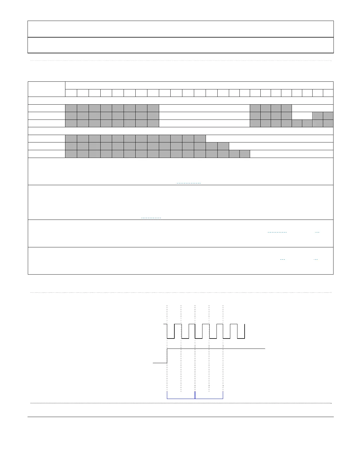
Figure 7
2X Clock timing
2
nd
edge
1
st
edge
2X CLK
DE
1
st
Pixel
Data On Input Bus
2
nd
Pixel
2
nd
edge
1
st
edge
 Loading...