ADV7511W HARDWARE USER’S GUIDE
Rev. A
Page 41
of 45
Rev A
SECTION 7: PCB LAYOUT RECOMMENDATIONS
7.1 Power Supply filtering
All of the ADV7511W supply domains are 1.8V with the exception of DVDD_3V which is 3.3V and need to remain as
noise-free as possible for the best operation. Power supply noise has a frequency component that affects performance,
and this is specified in Vrms terms. ▶Figure 22
shows the maximum allowable noise in the ADV7511W.
It is recommended to combine the four 1.8 volt power domains of the ADV7511W into 3 separate PCB power
domains as shown in ▶Figure 21
. An LC filter on the output of the power supply is recommended to attenuate the
noise and should be placed as close to the ADV7511W as possible. An effective LC filter for this is a 10 μH inductor
and a 10μF capacitor (see▶ Figure 21
). This filter scheme will reduce any noise component over 20KHz to effectively 0.
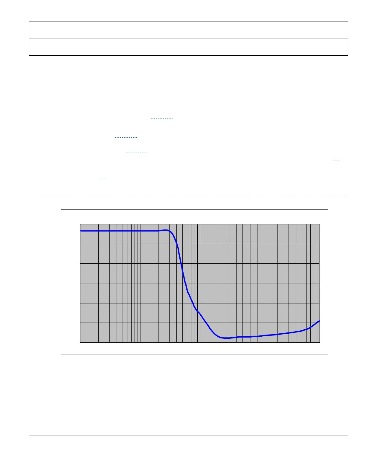
Using the recommended LC filter with realistic load and series resistance yields the transfer curve shown in Figure 23
.
Each of the power supply pins of the ADV7511W should also have a 0.1uF capacitor connected to the ground plane as
shown in Figure 21
. The capacitor should be placed as close to the supply pin as possible. Adjacent power pins can
share a bypass capacitor. The ground pins of the ADV7511W should be connected to the GND plane using vias.
Figure 22
AVDD and PVDD Max Noise vs. Frequency
Max rms noise vs frequency (DC to 10MHz)
0.0
5.0
10.0
15.0
20.0
25.0
30.0
1 10 100 1000 10000
frequency (KHz)
Max rms noise (mV)
 Loading...