ADV7511W HARDWARE USER’S GUIDE
Rev. A
Page 25
of 45
Rev A
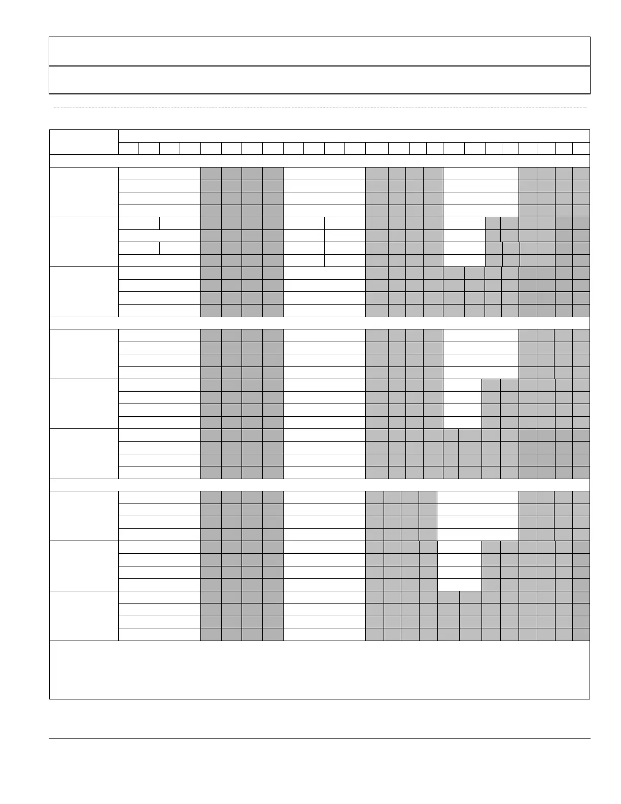
Table 10
YCbCr 4:2:2 (12, 10, 8 bits) DDR with Separate Syncs:Input ID = 6, evenly distributed (R0x48[4:3] = ‘00’)
Input Format
Data<23:0>
23 22 21 20 19 18 17 16 15 14 13 12 11 10 9 8 7 6 5 4 3 2 1 0
Style 1
YCrCb422 Sep
Syncs (DDR)
12 bit
Y[7:4]
Cb[3:0] Y[3:0]
Cb[11:8] Cb[7:4] Y[11:8]
Y[7:4] Cr[3:0] Y[3:0]
Cr[11:8] Cr[7:4] Y[11:8]
YCrCb422 Sep
Syncs (DDR)
10 bit
Y[5:4] Cb[3:2] Cb[1:0] Y[3:2] Y[1:0]
Cb[9:6] Cb[5:4] Y[9:8] Y[7:6]
Y[5:4] Cr[3:2] Cr[1:0] Y[3:2] Y[1:0]
Cr[9:6] Cr[5:4] Y[9:8] Y[7:6]
YCrCB 422
Sep. Syncs
(DDR)
8 bit
Cb[3:0]
Y[3:0]
Cb[7:4] Y[7:4]
Cr[3:0] Y[3:0]
Cr[7:4] Y[7:4]
Style 2
12 bit Y[11:8] Y[7:4] Y[3:0]
Cb[11:8] Cb[7:4] Cb[3:0]
Y[11:8] Y[7:4] Y[3:0]
Cr[11:8] Cr[7:4] Cr[3:0]
10 bit Y[9:6] Y[5:2] Y[1:0]
Cb[9:6] Cb[5:2] Cb[1:0]
Y[9:6] Y[5:2] Y[1:0]
Cr[9:6] Cr[5:2] Cr[1:0]
8 bit Y[7:4] Y[3:0]
Cb[7:4] Cb[3:0]
Y[7:4] Y[3:0]
Cr[7:4] Cr[3:0]
Style 3
12 bit Cb[11:8] Cb[7:4] Cb[3:0]
Y[11:8] Y[7:4] Y[3:0]
Cr[11:8] Cr[7:4] Cr[3:0]
Y[11:8] Y[7:4] Y[3:0]
10 bit Cb[9:6] Cb[5:2] Cb[1:0]
Y[9:6] Y[5:2] Y[1:0]
Cr[9:6] Cr[5:2] Cr[1:0]
Y[9:6] Y[5:2] Y[1:0]
8 bit Cb[7:4] Cb[3:0]
Y[7:4] Y[3:0]
Cr[7:4] Cr[3:0]
Y[7:4] Y[3:0]
An input format of YCbCr 4:2:2 DDR can be selected by setting the input ID (R0x15 [3:0]) to 0x6. The three different input pin assignment
styles are shown in the table. The Input Style can be set in R0x16[3:2]. The data bit width (12, 10, or 8 bits) must be set with R0x16 [5:4]. The
Data Input Edge is defined in R0x16 [1]. The 1
st
and the 2
nd
edge may be the rising or falling edge. The Data Input Edge is defined in R0x16 [1].
0b1 = 1
st
edge rising edge; 0b0 = 1
st
edge falling edge. Pixel 0 is the first pixel of the 4:2:2 word and should be where DE starts.
 Loading...