ADV7511W HARDWARE USER’S GUIDE
Rev. A
Page 37
of 45
Rev A
When the serial interface is inactive (SCL and SDA are high), communications are initiated by sending a start signal.
The start signal is a high-to-low transition on SDA while SCL is high. This signal alerts all slaved devices that a data
transfer sequence is coming.
The first eight bits of data transferred after a start signal comprise a seven bit slave address (the first seven bits) and a
single R/
W
bit (the eighth bit). The R/
W
bit indicates the direction of data transfer, read from (1) or write to (0) the
slave device. If the transmitted slave address matches the address of the device (set by the state of the A2 input pin as
shown in ▶Table 16
), the ADV7511W acknowledges by bringing SDA low on the 9th SCL pulse. If the addresses do
not match, the ADV7511W does not acknowledge.
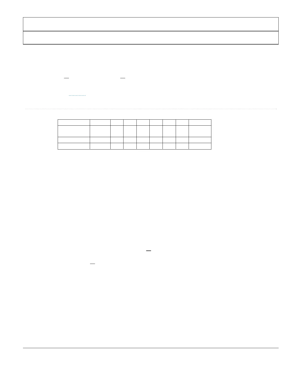
Table 16
Serial Port Addresses
Bit 7 Bit 6 Bit 5 Bit 4 Bit 3 Bit 2 Bit 1 Hex Addr.
PD/AD pin
Power-up state
A
6
(MSB) A
5
A
4
A
3
A
2
A
1
A
0
0 0 1 1 1 0 0 1 0x72
1 0 1 1 1 1 0 1 0x7A
6.6.2 Data Transfer via I2C
For each byte of data read or written, the most significant bit (MSB) is the first bit of the sequence.
If the ADV7511W does not acknowledge the master device during a write sequence, the SDA remains high so the
master can generate a stop signal. If the master device does not acknowledge the ADV7511W during a read sequence,
the ADV7511W interprets this as end of data. The SDA remains high, so the master can generate a stop signal.
Writing data to specific control registers of the ADV7511W requires that the 8-bit address of the control register of
interest be written after the slave address has been established. This control register address is the base address for
subsequent write operations, however, it is reset after a STOP command. The base address auto-increments by one for
each byte of data written after the data byte intended for the base address. If more bytes are transferred than there are
available addresses, the address does not increment and remains at its maximum value. Any base address higher than
the maximum value does not produce an acknowledge signal.
Data are read from the control registers of the ADV7511W in a similar manner. Reading requires two data transfer
operations:
1.
The base address must be written with the R/
W
bit of the slave address byte low to set up a sequential read
operation.
2.
Reading (the R/
W
bit of the slave address byte high) begins at the previously established base address. The
address of the read register auto-increments after each byte is transferred.
To terminate a read/write sequence to the ADV7511W, a stop signal must be sent. A stop signal comprises a low-to-
high transition of SDA while SCL is high. As in the write sequence, a STOP command resets the base address.
A repeated start signal occurs when the master device driving the serial interface generates a start signal without first
generating a stop signal to terminate the current communication. This is used to change the mode of communication
(read/write) between the slave and master without releasing the serial interface lines.
 Loading...