ADV7511W HARDWARE USER’S GUIDE
Rev.A
Page 18
of 45
Rev A
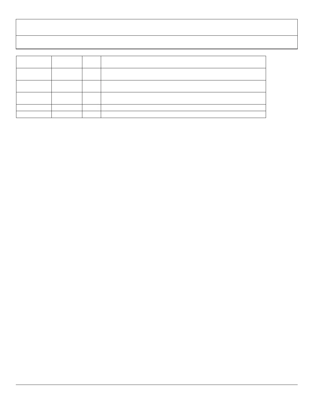
36 SDA C
Serial Port Data I/O. This pin serves as the serial port data I/O slave for register
access. Supports CMOS logic levels from 1.8V to 3.3V.
35 SCL C
Serial Port Data Clock input. This pin serves as the serial port data clock slave for
register access. Supports CMOS logic levels from 1.8V to 3.3V.
34 DDCSDA C
Serial Port Data I/O to Sink. This pin serves as the master to the DDC bus. Tolerant
of 5 V CMOS logic levels.
33 DDCSCL C
Serial Port Data Clock to Sink. This pin serves as the master clock for the DDC
bus. Tolerant of 5 V CMOS logic levels.
32 CEC_CLK I CEC clock. From 3MHz to 100Mhz. Supports CMOS logic levels from 1.8V to 5V.
30 CEC I/O CEC data signal. Supports CMOS logic levels from 1.8V to 5V.
1. I = input, O = output, P = power supply, C = control
 Loading...