Host Interface 34 (114)
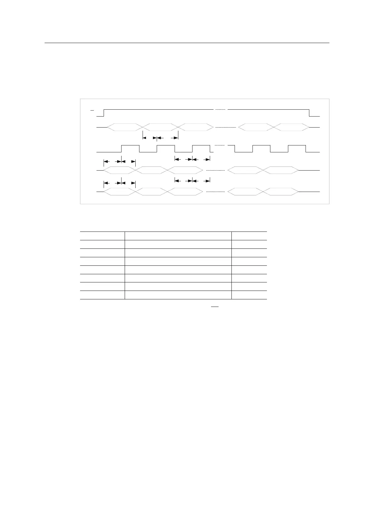
3.5.3 Timing
The Anybus CompactCom M40 operates in 12.5 MHz in shift register mode.
Timing Diagram
SCK
DI
DO
D7 D6 D5
D7 D6 D5
t
SUO
t
HDO
t
HDI
t
SUI
t
CH
LD
t
CL
D1 D0
D1 D0
CT
t
HDI
t
SUI
t
CH
t
CL
Fig. 17
Abbreviations from the diagram above, explained, and timing details:
Item Description Min Value
tSUO DO setup before SCK rising edge 20 ns
tHDO DO hold after SCK rising edge 20 ns
tSUI DI/CT setup before SCK rising edge 10 ns
tHDI DI/CT hold after SCK rising edge 0 ns
tCH SCK high period 35 ns
tCL SCK low period 35 ns
tCH + tCL SCK period 78 ns
The idle time between two transfers, i.e. when the LD signal is low, is at least 1 µs.
The cycle time range is typically 160 µs to 200 µs. However it is highly module and network
dependent, and may differ from the defined range.
Anybus
®
CompactCom
™
M40 Hardware Design Guide HMSI-216-126 EN 2.6