Appendix D: Mechanical Specification 88 (114)
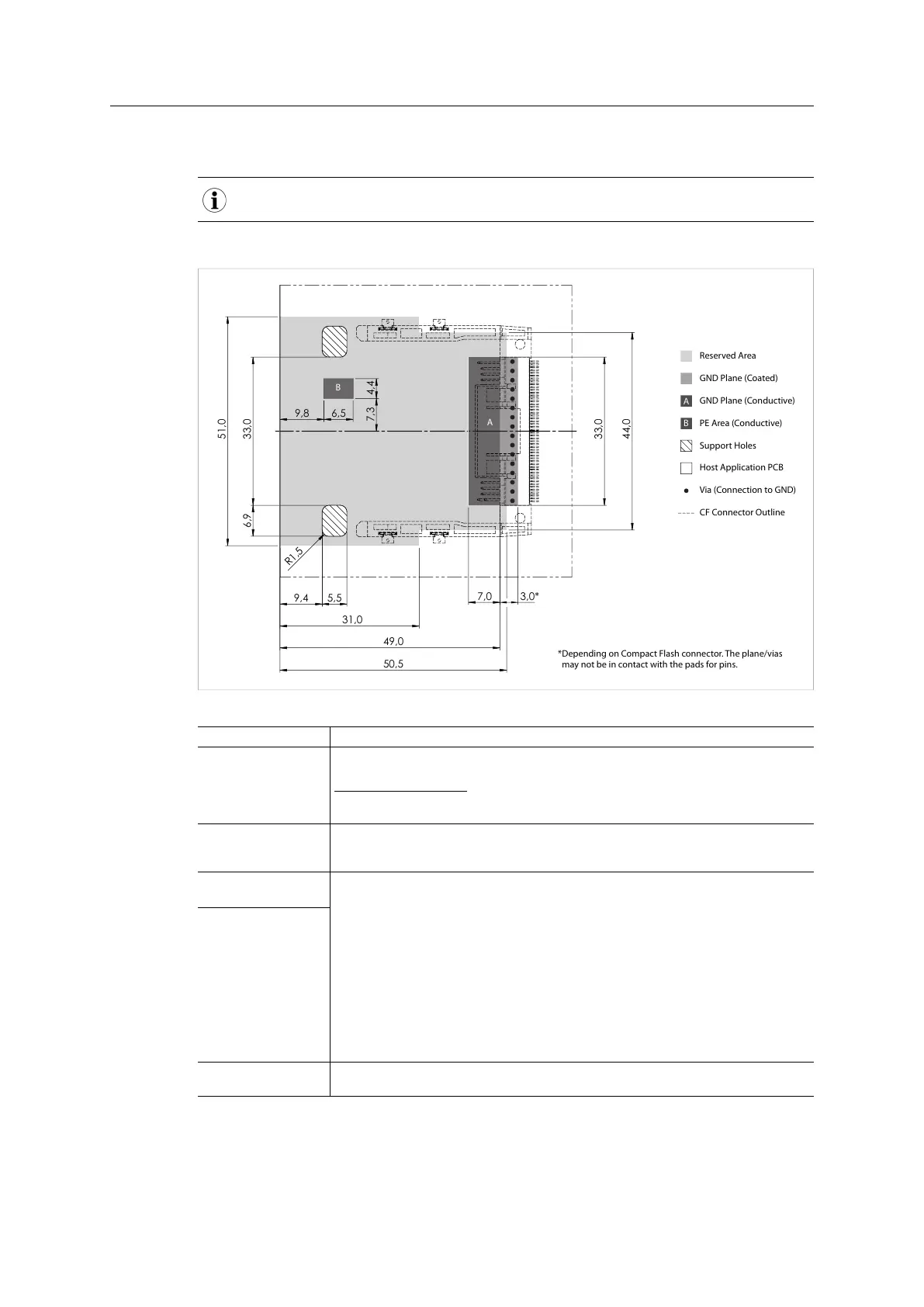
D.3 Footprint
The dimensions below are given in millimeters and include a tolerance of ±0.10 mm.
For a footprint for the Anybus CompactCom host connector, see Host Connector, p. 91
33,0
4,4
6,5
33,0
7,0
7,3
6,9
5,5
R
1,5
9,4
50,5
49,0
31,0
51,0
9,8
44,0
B
A
Reserved Area
GND Plane (Coated)
GND Plane (Conductive)
A
PE Area (Conductive)
B
Support Holes
Host Application PCB
Via (Connection to GND)
CF Connector Outline
3,0*
*Depending on Compact Flash connector. The plane/vias
may not be in contact with the pads for pins.
Fig. 39
Area Description
Reserved Area To ensure isolation and mechanical compatibility, it is strongly advised that this area is
kept completely free from components and signal lines.
Under no circumstances may components, via holes, or signal lines, be placed on the
PCB-layer facing the Anybus module. Failure to comply with this requirement may
induce EMC/EMI problems, mechanical compatibility issues, or even short circuit.
FE Area
(Conductive)
To achieve proper EMC behavior and to provide support for different cable shielding
standards, this area must be tin plated (preferably using Hot Air Levelling technology)
and have a stable, low impedance connection to functional earth.
GND Plane
(Coated)
The exact shape of this area depends on the properties of the CompactFlash connector.
It is however important to follow these basic design rules:
• The plane must be continuous and have a stable, low impedance connection to
GND (preferably through at least 16 vias as illustrated in the figure)
• The connection to GND should be placed beneath the CompactFlash connector as
illustrated above (see figure)
• The plane must follow the signal path through the connector
• The conductive part must be tin plated, preferably using Hot Air Levelling
technology
GND Plane
(Conductive)
Support Holes These holes are used by the fastening mechanics to secure the module onto the host
application.
Anybus
®
CompactCom
™
M40 Hardware Design Guide HMSI-216-126 EN 2.6