CYC5000 User Guide www.arrow.com
Page | 47 March 2023
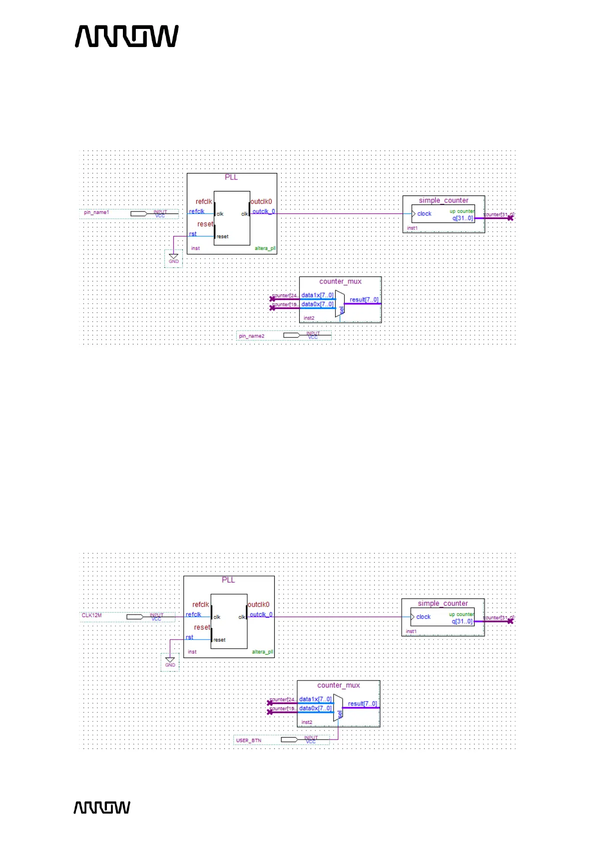
5.2.9.2 Add one input pin for refclk of the PLL and add other one input pin for sel of
counter_mux.
Your schematic should look like this:
5.2.9.3 Rename the pin_name1 to CLK12M by double clicking its current name. This is going to
be the clock signal coming into the FPGA.
5.2.9.4 Rename the pin_name2 to USER_BTN by double clicking its current name. This is going
to be one of the user buttons of the CYC5000 board to select the mux.
5.2.9.5 Using the “Node Tool” connect:
CLK12M → refclk (of the PLL component)
USER_BTN → sel (of the counter_mux component)
Your schematic should look like this now: