Copyright © 2016 ASIX Electronics Corporation. All rights reserved.
AX99100
PCIe to Multi I/O Controller
1.4.1 GPIO and Mode Setting
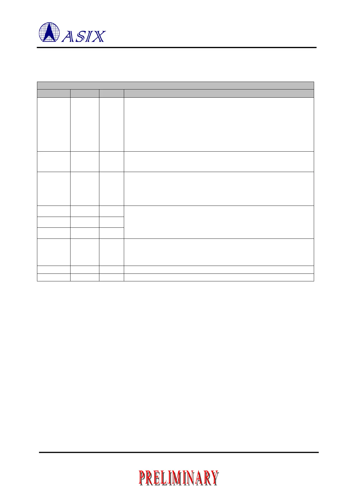
Table 1-4: GPIO and Mode Setting Pin Description
GPIO and Mode Setting Pins
31, 32,
33, 34,
38, 40,
41, 42,
43, 44,
45, 46,
47, 48,
49, 50
General Purpose I/O signal
GPIO[15:8] are only valid when CHIP_MODE = 100 and 110.
GPIO[23:16] are only valid when CHIP_MODE = 100 and 110 and Port 4 was
disabled by HWCFGEE. Please reference to Section 3.
General Purpose Output signal
GPIO7 has an optional function is external wakeup pin in input direction. When
AX99100 entered to L2 mode, this pin can be used to wakeup AX99100 also.
General Purpose Output signal
GPIO6 has an optional function is a power-down control signal to power down
the external transceiver when AX99100 entered to L2 mode. This function can be
enabled by setting bit1 and the polarity selection is bit0 in configuration
EEPROM, offset 0x55.
General Purpose Output signal when chip exited reset and operating in normal
functional mode.
These pins are input direction during chip reset use to bootstrap the mode setting
to decide the chip operation mode. Please reference to Section 3.1.
General Purpose Output signal when chip exited reset and operating in normal
functional mode.
This pin should be connected to the AUX 3.3V in PCIe slot via an external
pull-up resistor. It is used to detect the 3.3V AUX is existed or not.
General Purpose I/O signal
General Purpose I/O signal
Note: Above GPIO[7:0] are only valid when CHIP_MODE ≠ 000.
 Loading...
