EasyManuals Logo

ASIX AX99100 User Manual

Default Icon
70 pages
To Next Page IconTo Next Page
To Previous Page IconTo Previous Page
Page #49 background imageLoading...
Page #49 background image
49
AX99100
PCIe to Multi I/O Controller
Copyright © 2016 ASIX Electronics Corporation. All rights reserved.
PCIe Configuration Space Map 3.4
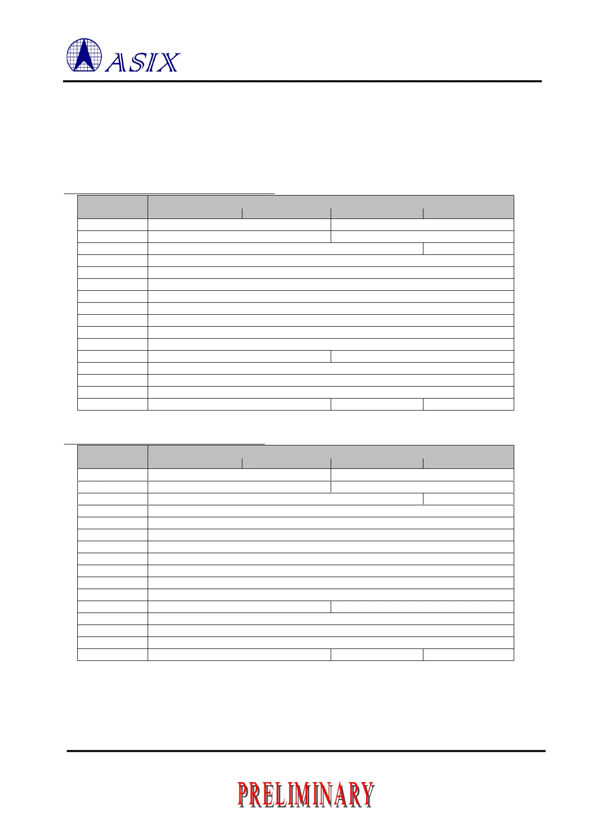
Following tables show the BAR usages in different interfaces. The detail function description, please reference in
PCIe base specification Revision 1.1. About the interrupt mapping in chip default, the function 0~3 will be mapped
to INTA~D.
PCI Configuration Space Map for SP (Function 0~3)
Offset
Register Name
31 24
23 16
15 8
7 0
0x00
Device ID
Vendor ID
0x04
Status
Command
0x08
Class Code
Revision ID
0x0C
0x10
Base Address Registers 0
0x14
Base Address Registers 1
0x18
0x1C
0x20
0x24
Base Address Registers 5
0x28
0x2C
Subsystem ID
Subsystem Vendor ID
0x30
0x34
0x38
0x3C
Interrupt Pin
Interrupt Line
PCI Configuration Space Map for PP (Function 2)
Offset
Register Name
31 24
23 16
15 8
7 0
0x00
Device ID
Vendor ID
0x04
Status
Command
0x08
Class Code
Revision ID
0x0C
0x10
Base Address Registers 0
0x14
Base Address Registers 1
0x18
Base Address Registers 2
0x1C
0x20
0x24
Base Address Registers 5
0x28
0x2C
Subsystem ID
Subsystem Vendor ID
0x30
0x34
0x38
0x3C
Interrupt Pin (0x03)
Interrupt Line

Table of Contents

Questions and Answers:

Question and Answer IconNeed help?

Do you have a question about the ASIX AX99100 and is the answer not in the manual?

ASIX AX99100 Specifications

General IconGeneral
BrandASIX
ModelAX99100
CategoryController
LanguageEnglish

Related product manuals