EasyManuals Logo

ASIX AX99100 User Manual

Default Icon
70 pages
To Next Page IconTo Next Page
To Previous Page IconTo Previous Page
Page #15 background imageLoading...
Page #15 background image
15
Copyright © 2016 ASIX Electronics Corporation. All rights reserved.
AX99100
PCIe to Multi I/O Controller
1.4.5 Serial Port with Function Disabled
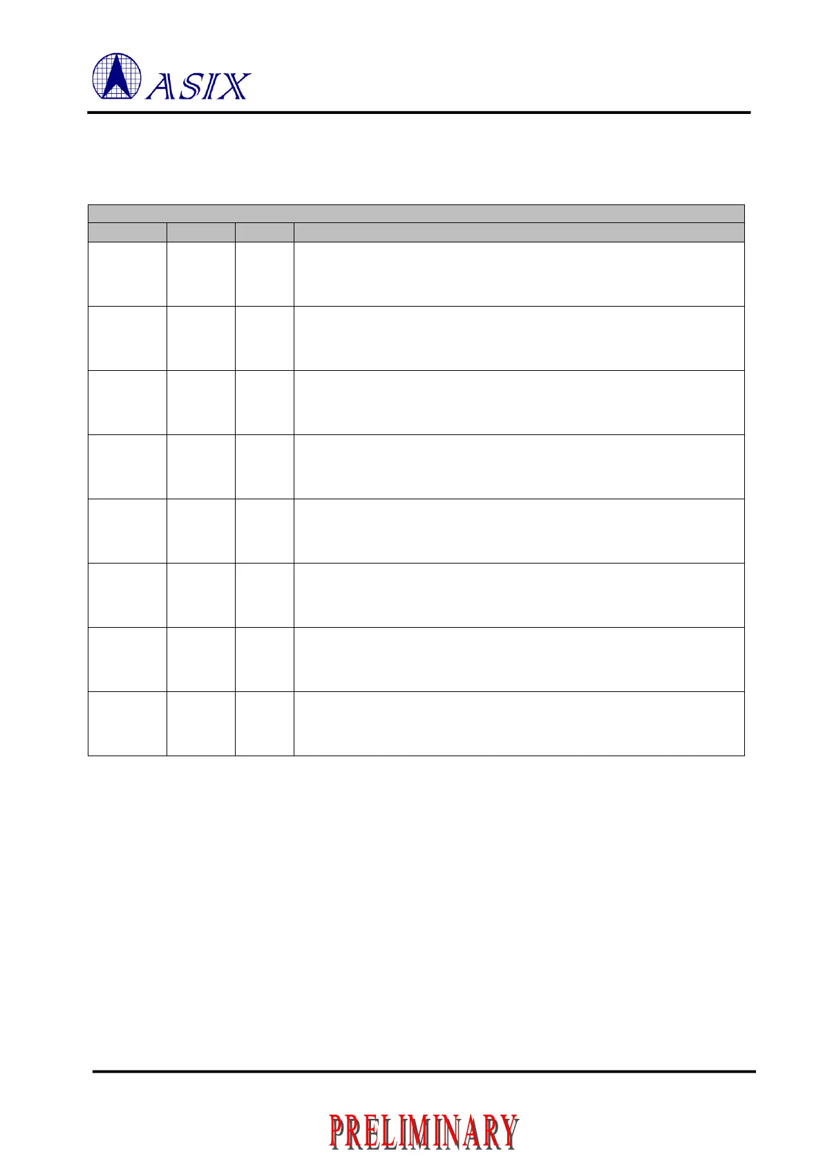
Table 1-8: Serial Interface with Port2 and Port4 Disabled Pin Description
Serial Interface with Port2 and Port4 Disabled
Pin Name
Type
Pin No
Pin Description
TXD2
TXD4
O5/4m
68
42
No any function for this pin due to disable.
SP1_GPIO0
SP3_GPIO0
B5/CU/4m
67
41
Serial Port GPIO
(Note 2)
SP1_GPIO1
SP3_GPIO1
B5/CU/4m
66
40
Serial Port GPIO
RXD2
RXD4
O5/PU/4m
65
38
No any function for this pin due to disable.
SP1_GPIO5
SP3_GPIO5
B5/CU/4m
64
34
Serial Port GPIO
SP1_GPIO3
SP3_GPIO3
B5/CU/4m
63
33
Serial Port GPIO
SP1_GPIO4
SP3_GPIO4
B5/CU/4m
62
32
Serial Port GPIO
SP1_GPIO2
SP3_GPIO2
B5/CU/4m
61
31
Serial Port GPIO
Note 1: If Port 2 or Port 4 are disabled by setting HWCFGEE when CHIP_MODE setting for those serial port
interface, all pins for Port 2 or Port 4 (excluded TXD and RXD) will be re-directed to the GPIO function of
Port 1 and Port 3. Thus the pins of Port 1 and Port 3 cannot be set for GPIO function by software register
setting.
Note 2: Pin 67 and 41 will be re-directed to DTR1/DXEN1 and DTR3/DXEN3 also. However software can enable it
to GPIO function as SP1_GPIO0 and SP3_GPIO0.

Table of Contents

Questions and Answers:

Question and Answer IconNeed help?

Do you have a question about the ASIX AX99100 and is the answer not in the manual?

ASIX AX99100 Specifications

General IconGeneral
BrandASIX
ModelAX99100
CategoryController
LanguageEnglish

Related product manuals