Copyright © 2016 ASIX Electronics Corporation. All rights reserved.
AX99100
PCIe to Multi I/O Controller
1.4.7 SPI Interface
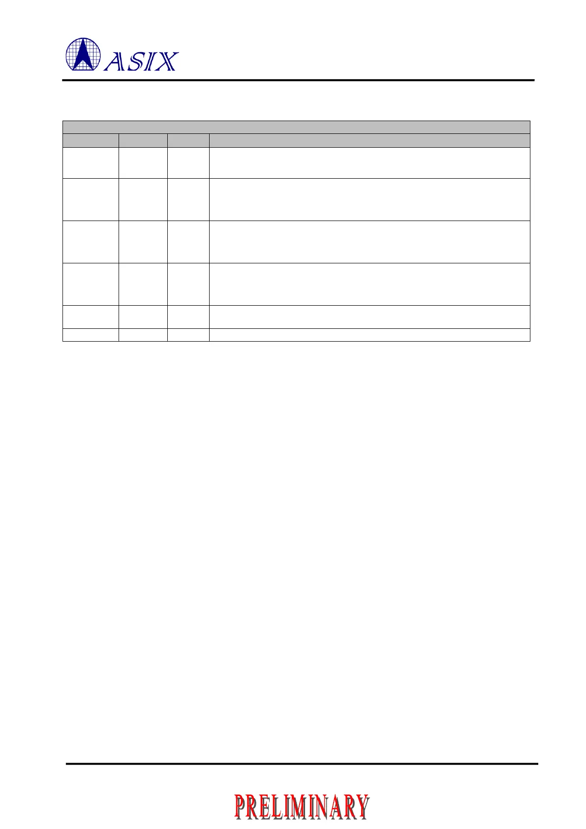
Table 1-10: SPI Pin Description
SPI Slave Select for SPI master.
SS[2:0] is a tri-stateable output, which requires an external pull-up resistor.
SPI CLocK for SPI master.
SCLK is a tri-stateable output. At Mode 0 or 2, SCLK requires external pull-down
resistor; while at Mode 1 or 3, SCLK requires external pull-up resistor.
SPI Master Output Slave Input line for SPI master.
When High Speed SPI controller is operating in master module, MOSI is used to
transmit serial data and is a tri-stateable output.
SPI Master Input Slave Output line for SPI master.
When High Speed SPI controller is operating in master module, MISO is used to
receive serial data.
SPI External Wakeup
SWAKEn is external wakeup for SPI interface.
General Purpose I/O signal
Note: Above signals are only valid when CHIP_MODE = 100 and 110.
 Loading...
