AX99100
PCIe to Multi I/O Controller
Copyright © 2016 ASIX Electronics Corporation. All rights reserved.
4.5.3 Serial Port Timing
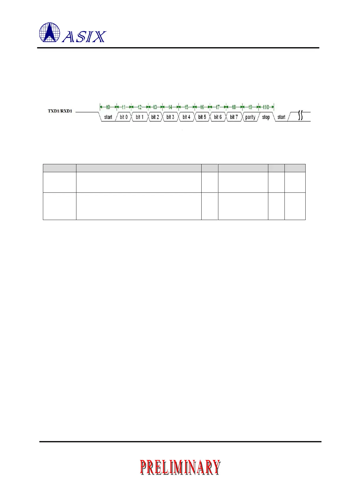
The Serial Port data transmit and receive is via TXD[4:1] and RXD[4:1] pins. The complete data transmit/receive
includes 1 start bit, 5~8 data bit, 1 parity bit (if supported parity check) and 1~2 stop bit.
Figure 4-1: TXD1 and RXD1 Timing Diagram
t0 is start bit time;
t1 ~ t8 is data bit time;
t9 is parity bit time;
stop bit time :
1 bit
1.5 bit
2 bit
1/Baud Rate
1.5*(1/Baud Rate)
2*(1/Baud Rate)
Note: RXD[4:1] baud rate tolerance ±3%.
 Loading...
