Copyright © 2016 ASIX Electronics Corporation. All rights reserved.
AX99100
PCIe to Multi I/O Controller
Signal Description 1.4
Following abbreviations are used in “Type” column of following pin description tables. Note that some I/O pins with
multiple signal definitions on the same pin may have different attribute in “Type” column for different signal
definition.
Analog Bi-directional I/O
Output, 3.3V with 5V tolerant
Analog Output
Bi-directional I/O, 3.3V
Internal Pull-Down (75K)
Controllable internal Pull-Up
Bi-directional I/O, 3.3V with 5V tolerant
Power and ground pin
Schmitt Trigger
Input, 3.3V with 5V tolerant
For example, pin 5 in AX99100 package can be RXD1 or AD3. If RXD1 is selected, its Type is I5/PU; if AD3 is
selected, its Type is B5/4m. In other words, the PU (internal pull-up) only takes effect in RXD1 signal mode while
AD3 signal mode doesn’t. User should refer to the table specific to desired function for exact pin type definition.
The multi-function pin settings are configured by pin 54, 56 and 58 to decide the chip operating mode. Please
reference to Section 3 in detailed. The following abbreviations are used in pin description tables.
HWCFGEE I
2
C Hardware Configuration EEPROM
CHIP_MODE Chip Operating Mode, Setting by external pull the pin 54, 56 and 68
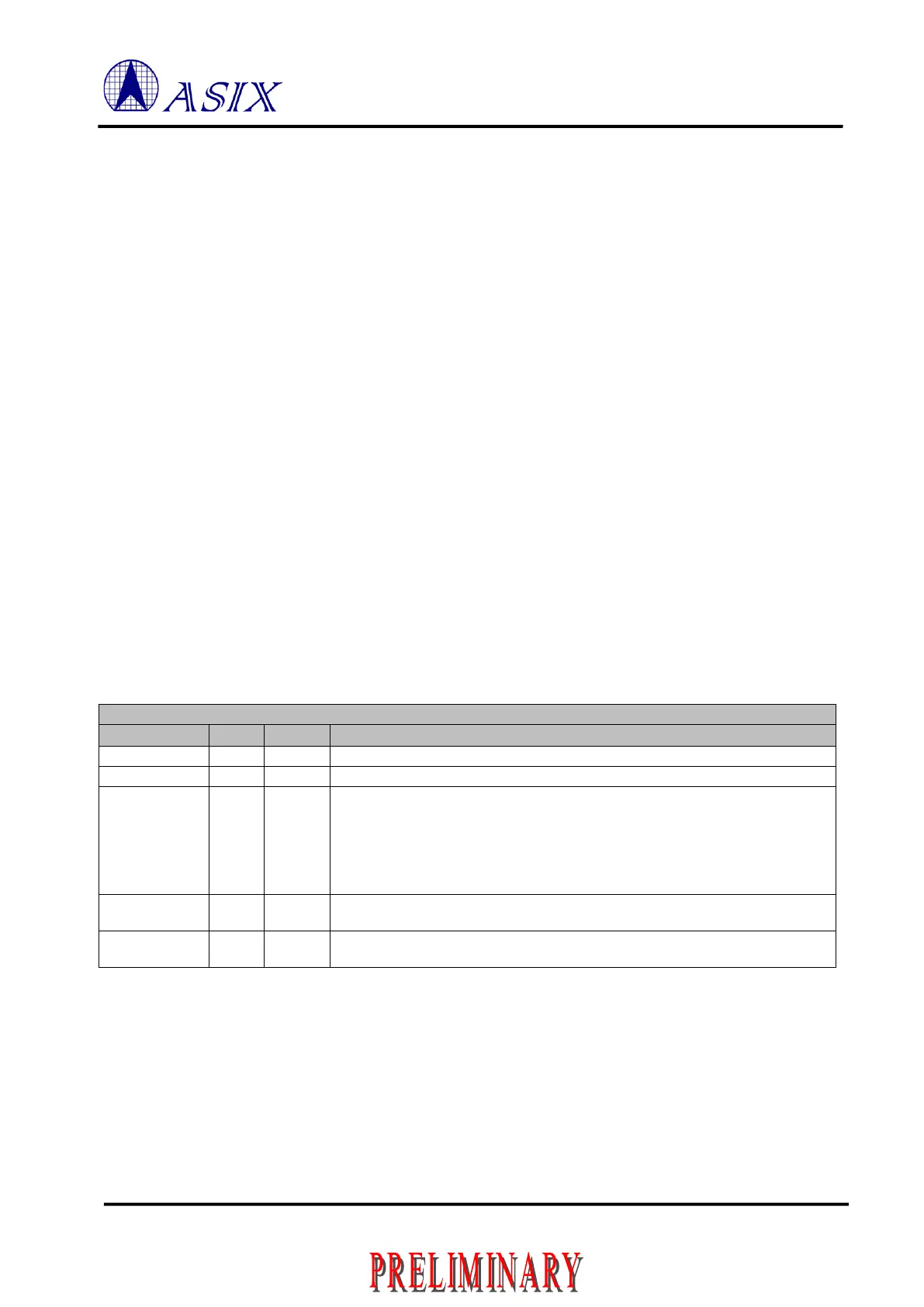
Table 1-1: Common Pin Description
Test Mode enable. For normal operation, please always tie to logic low or NC.
External Clock Input from external Oscillator.
External Clock Power Down enable.
0: Power down external Oscillator.
1: Enable external Oscillator.
Note: When external Oscillator existed, this pin should be pull down by external
resistor for boot strapping latch. Otherwise, please pull-up by external
resistor to indicate NO external Oscillator existed.
I
2
C Serial Clock line for I
2
C master controller.
SCL is a tri-stateable output, which requires an external pull-up resistor.
I
2
C Serial Data line for I
2
C master controller.
SDA is a tri-stateable output, which requires an external pull-up resistor.
 Loading...
