AX99100
PCIe to Multi I/O Controller
Copyright © 2016 ASIX Electronics Corporation. All rights reserved.
AC Timing Characteristics 4.5
4.5.1 PCIe Reference Clock Timing
The reference clock (CLKP and CLKN) of AX99100 is designed for the PCI Express Card Electromechanical
Specification Revision 2.0. Please reference the section 2.1.3 in this standard for the detail.
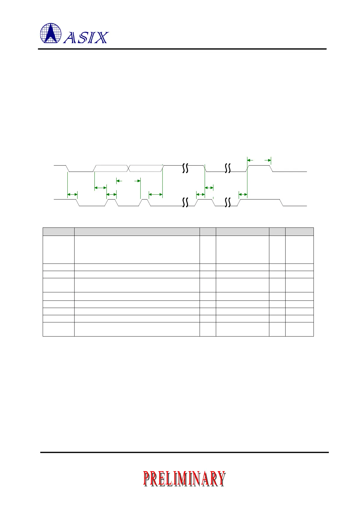
4.5.2 I
2
C Timing
SCL clock frequency
SCL will use 100KHz during the configuration
EEPORM loading and can be changed to support
400KHz operating.
High period of the SCL clock
Low period of the SCL clock
Hold time of (repeated) START condition. After
this period, the first clock pulse is generated
Setup time for a repeated START condition
Setup time for STOP condition
Bus free time between a STOP and START
condition
Note 1: Tsys_clk = 16ns for 62.5 MHz operating system clock.
Note 2: Fclk = 1/Tclk, where Tclk = ((SCL_HP + SCL_LP) * Tsys_clk). The SCL_HP and SCL_LP are I
2
C SCL
Period Register.
Table 4-1: I
2
C Master Controller Timing Table
Tsu_sto
Thd_sta
Tsu_staThd_dat
Tlow
Thigh
Tlow
Tsu_dat
ThighThd_sta
TbufTbuf
 Loading...
