AX99100
PCIe to Multi I/O Controller
Copyright © 2016 ASIX Electronics Corporation. All rights reserved.
4 Electrical Specifications
DC Characteristics 4.1
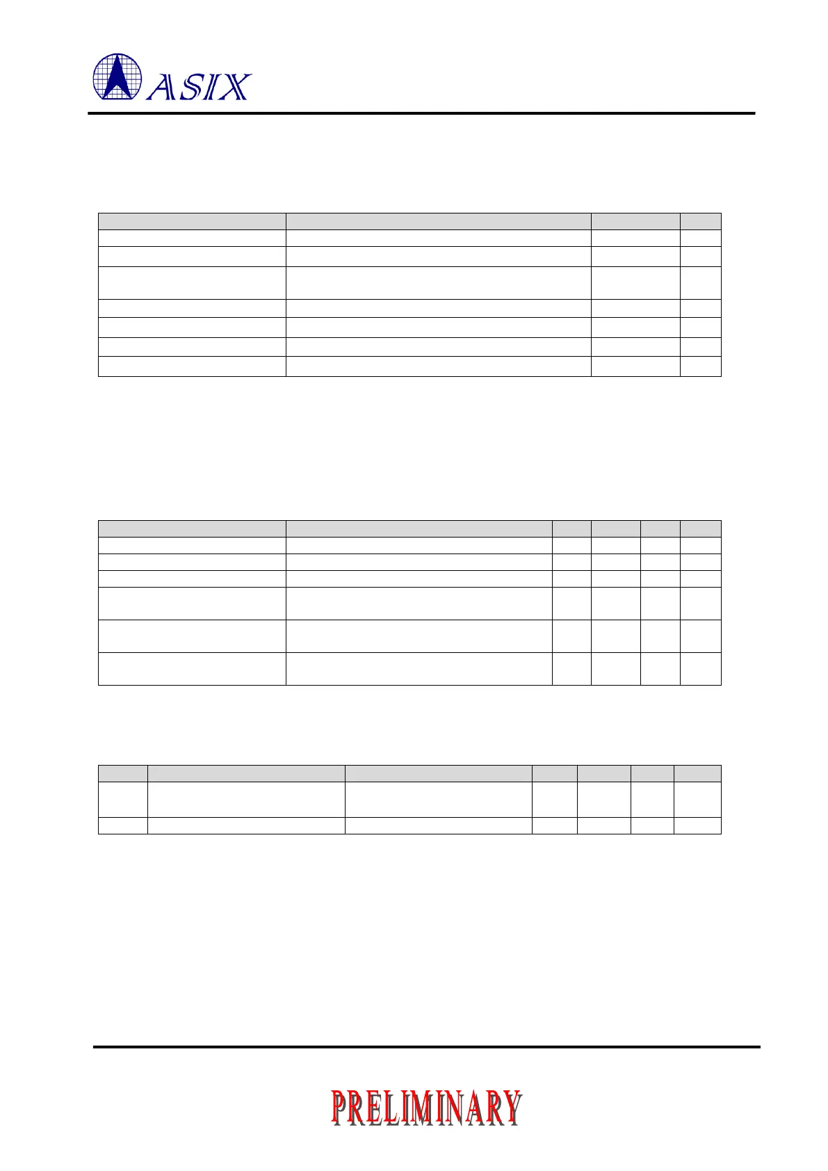
4.1.1 Absolute Maximum Ratings
Digital core power supply.
Power supply of 3.3V I/O and Regulator.
VCC12A_TX, VCC12A_AUX,
VCC12A_D
Analog power supply for PCIe PHY.
Input voltage of 3.3V I/O with 5V tolerant.
Output short circuit current.
Note:
Permanent device damage may occur if absolute maximum ratings are exceeded. Functional operation should be
restricted in the recommended operating condition section of this datasheet. Exposure to absolute maximum rating
condition for extended periods may affect device reliability.
4.1.2 Recommended Operating Condition
Power supply of 3.3V I/O.
Digital core power supply.
Analog power supply for Regulator.
VCC12A_TX, VCC12A_AUX,
VCC12A_D
Analog power supply for PCIe PHY.
AX99100 QF operating junction temperature.
AX99100 QI operating junction temperature.
AX99100 QF operating ambient temperature.
AX99100 QI operating ambient temperature.
4.1.3 Leakage Current and Capacitance
Input leakage current. No pull-up
or pull-down.
3.3V with 5V tolerant I/O pins.
Vin = 5 or 0V.
3.3V with 5V tolerant I/O pins.
 Loading...
