AX99100
PCIe to Multi I/O Controller
Copyright © 2016 ASIX Electronics Corporation. All rights reserved.
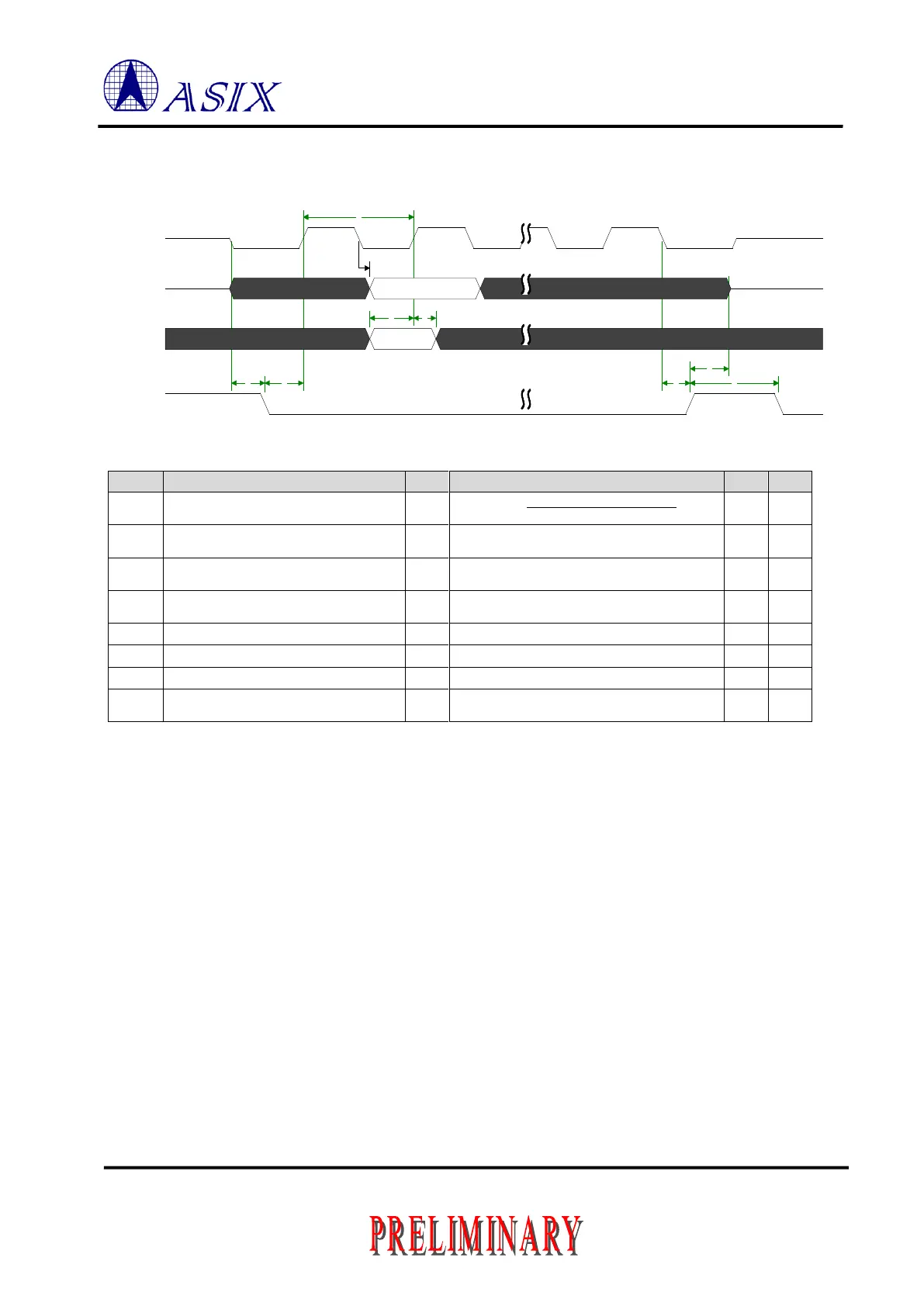
4.5.4 SPI Timing
Setup time of SS[2:0] to the first SCLK
edge
Mode0, 1: (1.0 + DBS) * Tsclk.
Mode2, 3: (0.5 + DBS) * Tsclk.
Hold time of SS[2:0] after the last SCLK
edge
Mode0, 1: (0.5 + DBS) * Tsclk.
Mode2, 3: (1.0 + DBS) * Tsclk.
Minimum idle time between transfers
(minimum SS[2:0] high time)
MOSI data valid time, after SCLK edge
MISO data setup time before SCLK edge
MISO data hold time after SCLK edge
Bus drive time before SS[2:0] assertion
and after SS[2:0] de-assertion
Note: Fsys_clk is from 125MHz, 100MHz or EXT_CLK and the SCLK frequency is same as “Desired clock
frequency”. Please reference section 3.3.1, Divide Register. The SPIBRR is SPI Baud Rate Register and same
as N.
Figure 4-2: High Speed SPI Master Controller Timing Diagram and Table
SCLK(output)
MOSI(output)
MISO(input)
SS0(output)
 Loading...
