Copyright © 2016 ASIX Electronics Corporation. All rights reserved.
AX99100
PCIe to Multi I/O Controller
1.4.2 Serial Interface for COM Port
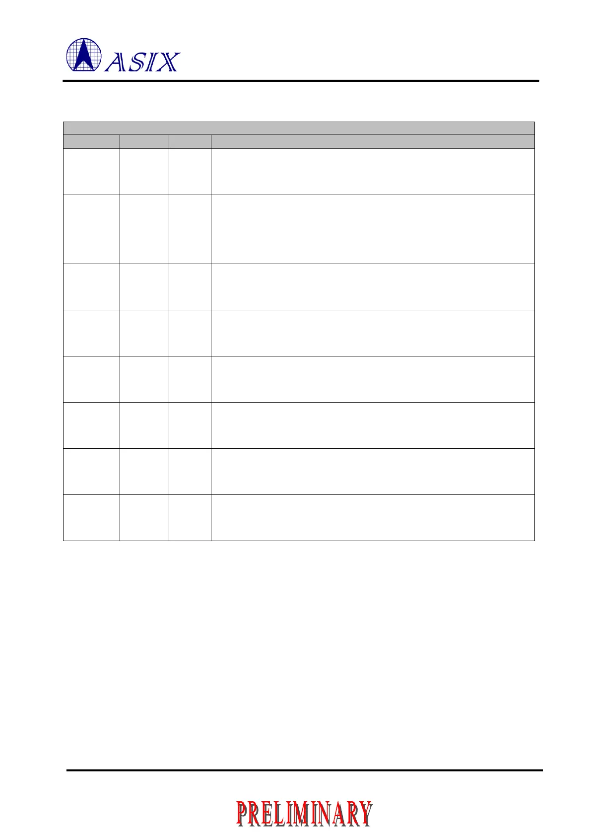
Table 1-5: Serial Interface for COM Port Pin Description
Serial Interface for COM Port
Transmit data output to transceiver or IrDA data output to IR LED
Data Terminal Ready
These pins have internal pull-down during reset. If there is the external pull-up
resisters connected to these pins separately, it will work for RS-232 function with
active low. Otherwise, it will work for RS-485 function (DXEN) with active high
and the output can be enabled by register (the default is disabled). Please
reference to Section 3.2.
Request to send (Active Low)
Note: These pins will be changed to RXEN when Software enabled RS-485
function for the corresponding ports.
Serial received data input from transceiver or IrDA data input from IrDA
detector.
Ring Indicator (Active Low)
Data Set Ready (Active Low)
Data Carrier Detect (Active Low)
Clear to send (Active Low)
Note 1: Serial Port 1 and 2 are only valid when CHIP_MODE = 001, 011, 101 and 110.
Note 2: Serial Port 3 and 4 are only valid when CHIP_MODE = 011.
 Loading...
