110
ATtiny26(L)
1477G–AVR–03/05
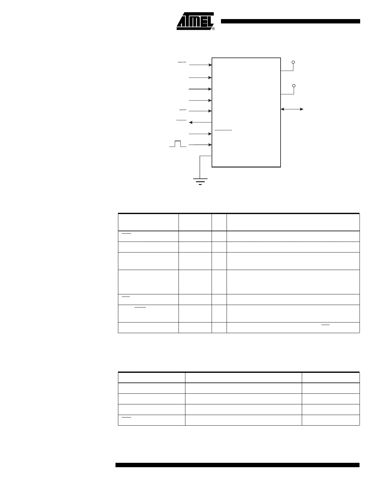
Figure 58. Parallel Programming
Note: 1. The pin is used for two different control signals. In the description below, normally
only one of the signals is referred. E.g., “give BS1 a positive pulse” equals “give
PAGEL/BS1 a positive pulse”.
Table 54. Pin Name Mapping
Signal Name in
Programming Mode Pin Name I/O Function
WR
PB0 I Write Pulse (Active low)
XA0 PB1 I XTAL Action Bit 0
XA1/BS2
(1)
PB2 I
XTAL Action Bit 1 multiplexed with Byte Select 2
(“0” selects low byte, “1” selects 2’nd high byte)
PAGEL/BS1
(1)
PB3 I
Program Memory and EEPROM data Page Load
multiplexed with Byte Select 1 (“0” selects low
byte, “1” selects high byte).
OE
PB5 I Output Enable (Active low)
RDY/BSY
PB6 O
0: Device is busy programming, 1: Device is ready
for new command
DATA PA7:0 I/O Bidirectional Data bus (Output when OE
is low)
Table 55. Pin Values used to Enter Programming Mode
Pin Symbol Value
PAGEL/BS1 Prog_enable[3] 0
XA1/BS2 Prog_enable[2] 0
XA0 Prog_enable[1] 0
WR
Prog_enable[0] 0
VCC
+5V
GND
XTAL1/PB4
PB0
PB1
PB2
PB3
PB5
PA7: PA0 DAT
RESET
PB6
+12 V
XA0
OE
RDY/BSY
AGEL/BS1
WR
XA1/BS2
AVCC
+5V