55
ATtiny26(L)
1477G–AVR–03/05
Notes: 1. Enabling of the Timer/Counter1 Compare match outputs and Timer/Counter1 PWM Outputs OC1A/OC1B and OC1A/OC1B
are described in the section “8-bit Timer/Counter1” on page 67.
2. Note that the PCINT0 Interrupt is only enabled if both the Global Interrupt Flag is enabled, the PCIE0 flag in GIMSK is set
and the alternate function of the pin is disabled as described in “Pin Change Interrupt” on page 62.
3. The Two-wire and Three-wire USI-modes are described in “Universal Serial Interface – USI” on page 80.
4. Shift clock (SCL) hold for USI is in described “Universal Serial Interface – USI” on page 80.
5. USI start up interrupt is enabled if both the Global Interrupt Flag is enabled and the USISIE flag in the USICR Register is set
as described in “Universal Serial Interface – USI” on page 80.
6. Data Output (DO) is valid in USI Three-wire mode and the operation is described in “Universal Serial Interface – USI” on
page 80.
7. Operation of the data pin SDA in USI Two-wire mode and DI in USI Three-wire mode in “Universal Serial Interface – USI” on
page 80.
8. Not operator is marked with “~”.
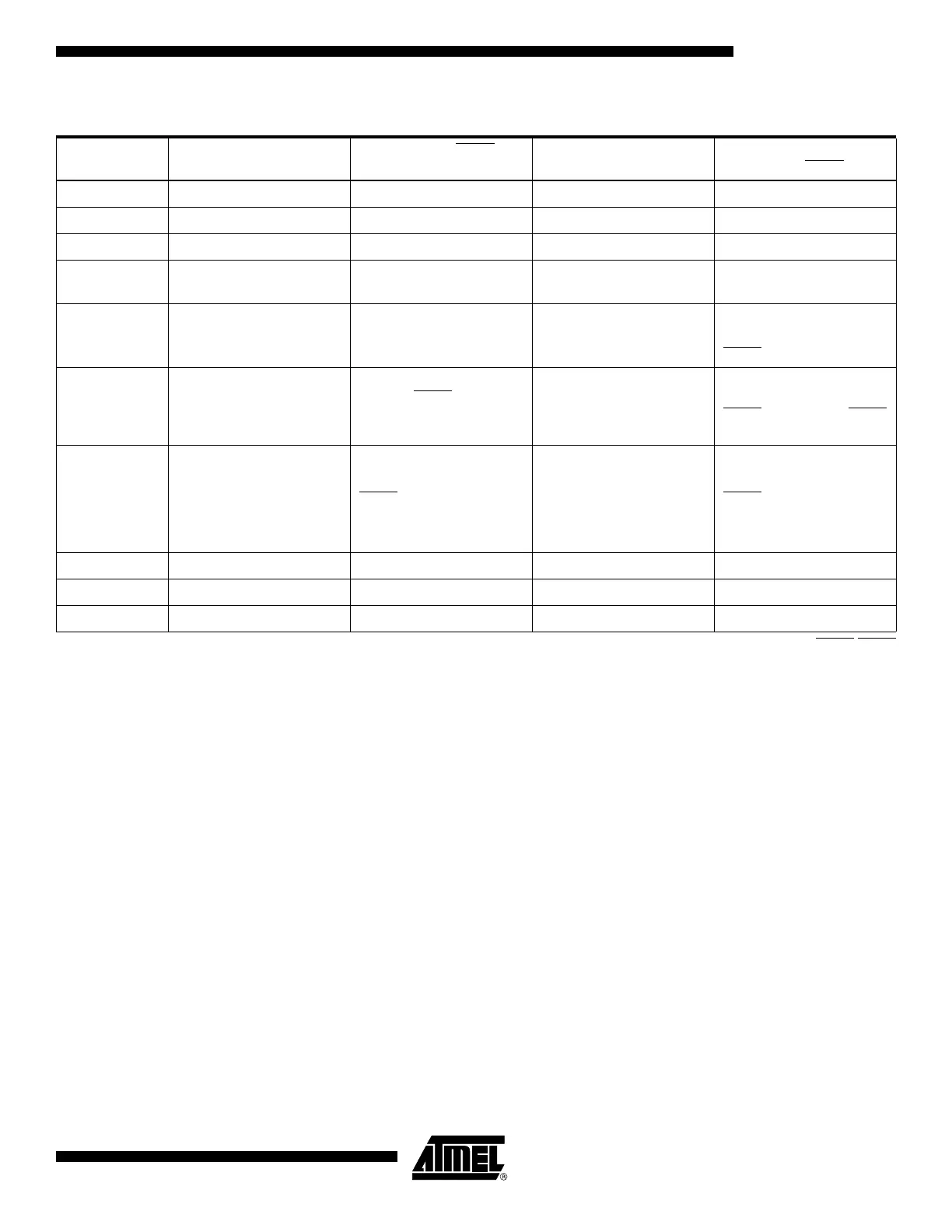
Table 28. Overriding Signals for Alternate Functions in PB3..PB0
Signal Name PB3/OC1B/PCINT0
PB2/SCK/SCL/OC1B
/PCI
NT0 PB1/DO/OC1A/PCINT0 PB0/DI/SDA/OC1A
PUOE 0 USI_TWO-WIRE
(3)
0 USI_TWO-WIRE
(3)
PUOV0000
DDOE 0 USI_TWO-WIRE
(3)
0USI_TWO-WIRE
(3)
DDOV 0 (USI_SCL_HOLD
(4)
|
~
(8)
PORTB2) • DDB2
0 (~SDA | ~PORTB0) •
DDB0
PVOE OC1B_ENABLE
(1)
USI_TWO-WIRE
(3)
•
DDB2 | OC1B_ENABLE
(1)
USI_THREE-WIRE
(3)
|
OC1A_ENABLE
(1)
USI_TWO-WIRE
(3)
• DDB0
|
OC1A
_ENABLE
(1)
PVOV OC1B ~(USI_TWO-WIRE •
DDB2) • OC1B
USI_THREE-WIRE
(3)
•
DO
(6)
| ~USI_THREE-
WIRE • OC1A_ENABLE
(1)
• OC1A
~(USI_TWO-WIRE•
DDB0) •
OC1A_ENABLE
(1)
• OC1A
DIEOE PCINT0_ENABLE
(2)
•
~OC1B_ENABLE
(1)
~(USI_TWO-WIRE |
USI_THREE-WIRE |
OC1B
_ENABLE) •
PCINT0_ENABLE
(2)
|
USI_START_I.ENABLE
(5)
~(USI_THREE-WIRE |
OC1A_ENABLE) •
PCINT0_ENABLE
(2)
~(USI_TWO-WIRE
(3)
|
USI_THREE-WIRE
(3)
|
OC1A
_ENABLE
(1)
) •
PCINT0_ENABLE
(2)
|
USI_START_I.ENABLE
(5)
DIEOV1111
DI PCINT0 PCINT0, SCL, SCK PCINT0 PCINT0, SDA
AIO––––