70
ATtiny26(L)
1477G–AVR–03/05
Timer/Counter1 Control
Register A – TCCR1A
• Bits 7, 6 – COM1A1, COM1A0: Comparator A Output Mode, Bits 1 and 0
The COM1A1 and COM1A0 control bits determine any output pin action following a
Compare Match with Compare Register A in Timer/Counter1. Output pin actions affect
pin PB1 (OC1A). Since this is an alternative function to an I/O port, the corresponding
direction control bit must be set (one) in order to control an output pin. Note that OC1A
is
not connected in normal mode.
In PWM mode, these bits have different functions. Refer to Table 35 on page 75 for a
detailed description.
• Bits 5, 4 – COM1B1, COM1B0: Comparator B Output Mode, Bits 1 and 0
The COM1B1 and COM1B0 control bits determine any output pin action following a
Compare Match with Compare Register B in Timer/Counter1. Output pin actions affect
pin PB3 (OC1B). Since this is an alternative function to an I/O port, the corresponding
direction control bit must be set (one) in order to control an output pin. Note that OC1B
is
not connected in normal mode.
In PWM mode, these bits have different functions. Refer to Table 35 on page 75 for a
detailed description.
• Bit 3 – FOC1A: Force Output Compare Match 1A
Writing a logical one to this bit forces a change in the Compare Match output pin PB1
(OC1A) according to the values already set in COM1A1 and COM1A0. If COM1A1 and
COM1A0 written in the same cycle as FOC1A, the new settings will be used. The Force
Output Compare bit can be used to change the output pin value regardless of the timer
value. The automatic action programmed in COM1A1 and COM1A0 takes place as if a
compare match had occurred, but no interrupt is generated. The FOC1A bit always
reads as zero. FOC1A is not in use if PWM1A bit is set.
• Bit 2 – FOC1B: Force Output Compare Match 1B
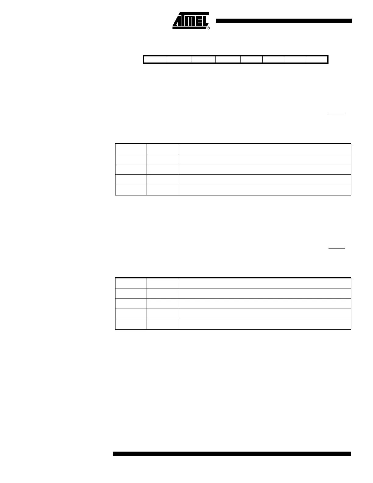
Bit 7 6 5 4 3 2 1 0
$30 ($50)
COM1A1 COM1A0 COM1B1 COM1B0 FOC1A FOC1B PWM1A PWM1B TCCR1A
Read/Write R/W R/W R/W R/W R/W R/W R/W R/W
Initial Value 0 0 0 0 0 0 0 0
Table 32. Comparator A Mode Select
COM1A1 COM1A0 Description
0 0 Timer/Counter Comparator A disconnected from output pin OC1A.
0 1 Toggle the OC1A output line.
1 0 Clear the OC1A output line.
1 1 Set the OC1A output line.
Table 33. Comparator B Mode Select
COM1B1 COM1B0 Description
0 0 Timer/Counter Comparator B disconnected from output pin OC1B.
0 1 Toggle the OC1B output line.
1 0 Clear the OC1B output line.
1 1 Set the OC1B output line.
 Loading...


