72
ATtiny26(L)
1477G–AVR–03/05
• Bits 3..0 – CS13, CS12, CS11, CS10: Clock Select Bits 3, 2, 1, and 0
The Clock Select bits 3, 2, 1, and 0 define the prescaling source of Timer/Counter1.
The Stop condition provides a Timer Enable/Disable function.
Timer/Counter1 – TCNT1
This 8-bit register contains the value of Timer/Counter1.
Timer/Counter1 is realized as an up counter with read and write access. Due to syn-
chronization of the CPU, Timer/Counter1 data written into Timer/Counter1 is delayed by
one CPU clock cycle in synchronous mode and at most two CPU clock cycles for asyn-
chronous mode.
Timer/Counter1 Output
Compare RegisterA – OCR1A
The Output Compare Register A is an 8-bit read/write register.
The Timer/Counter Output Compare Register A contains data to be continuously com-
pared with Timer/Counter1. Actions on compare matches are specified in TCCR1A. A
compare match does only occur if Timer/Counter1 counts to the OCR1A value. A soft-
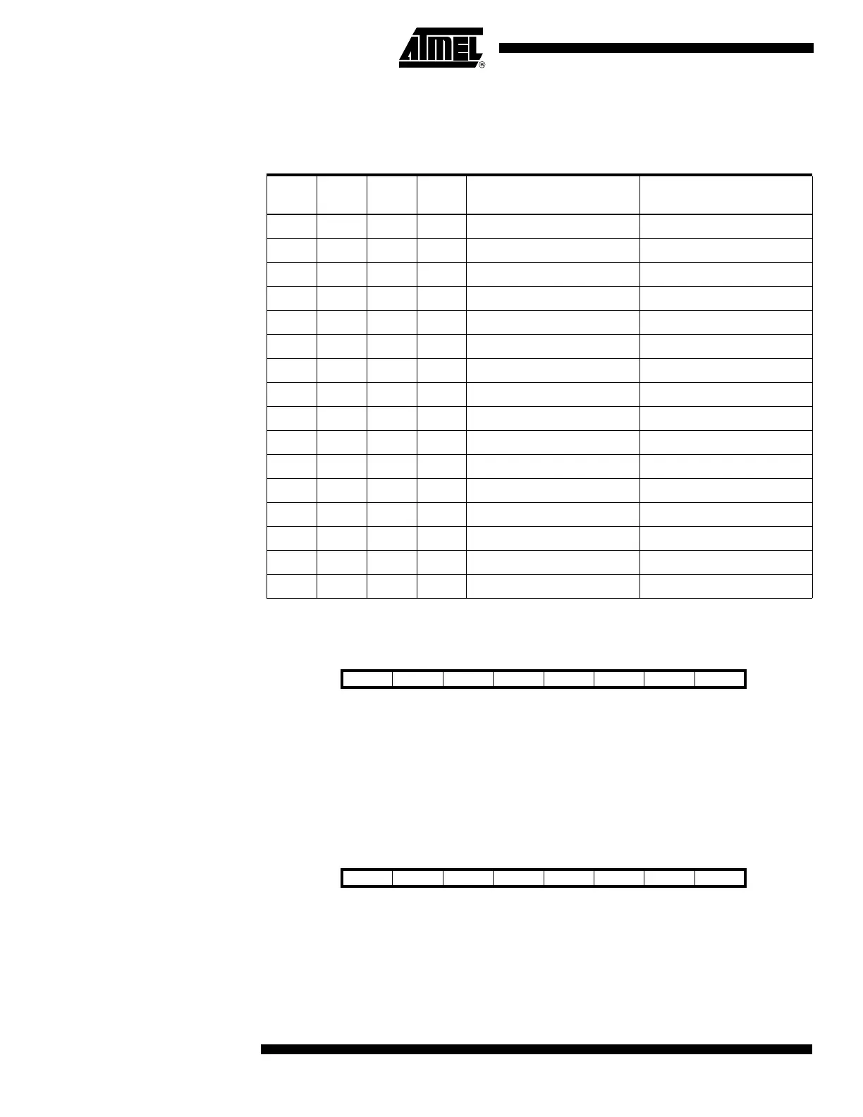
Table 34. Timer/Counter1 Prescale Select
CS13 CS12 CS11 CS10
Description
Asynchronous Mode
Description
Synchronous Mode
0000Timer/Counter1 is stopped.Timer/Counter1 is stopped.
0001PCK CK
0010PCK/2 CK/2
0011PCK/4 CK/4
0100PCK/8 CK/8
0101PCK/16 CK/16
0110PCK/32 CK/32
0111PCK/64 CK/64
1000PCK/128 CK/128
1001PCK/256 CK/256
1010PCK/512 CK/512
1011PCK/1024 CK/1024
1100PCK/2048 CK/2048
1101PCK/4096 CK/4096
1110PCK/8192 CK/8192
1111PCK/16384 CK/16384
Bit 76543210
$2E ($4E) MSB LSB TCNT1
Read/Write R/W R/W R/W R/W R/W R/W R/W R/W
Initial Value 0 0 0 0 0 0 0 0
Bit 76543210
$2D ($4D) MSB LSB OCR1A
Read/Write R/W R/W R/W R/W R/W R/W R/W R/W
Initial Value 0 0 0 0 0 0 0 0