Rev. 1.00
- 43 -
SRP-F310/312
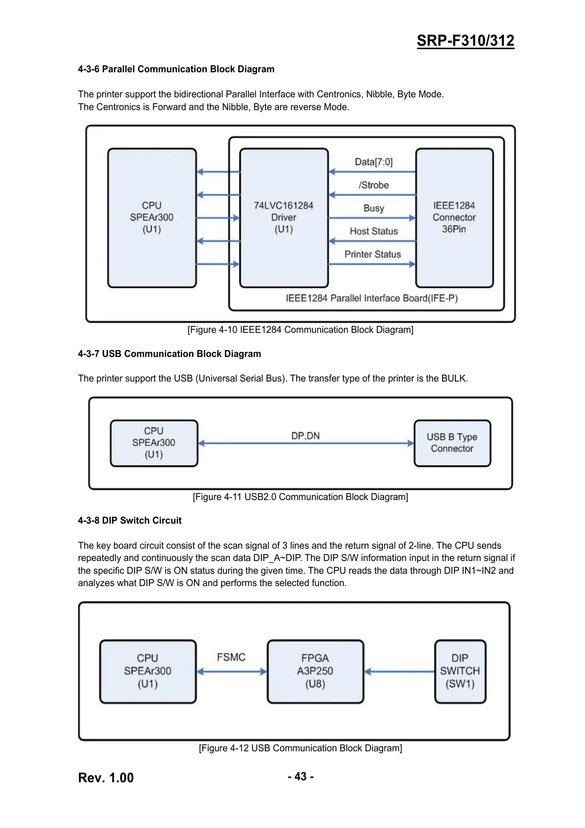
4-3-6 Parallel Communication Block Diagram
The printer support the bidirectional Parallel Interface with Centronics, Nibble, Byte Mode.
The Centronics is Forward and the Nibble, Byte are reverse Mode.
[Figure 4-10 IEEE1284 Communication Block Diagram]
4-3-7 USB Communication Block Diagram
The printer support the USB (Universal Serial Bus). The transfer type of the printer is the BULK.
[Figure 4-11 USB2.0 Communication Block Diagram]
4-3-8 DIP Switch Circuit
The key board circuit consist of the scan signal of 3 lines and the return signal of 2-line. The CPU sends
repeatedly and continuously the scan data DIP_A~DIP. The DIP S/W information input in the return signal if
the specific DIP S/W is ON status during the given time. The CPU reads the data through DIP IN1~IN2 and
analyzes what DIP S/W is ON and performs the selected function.
[Figure 4-12 USB Communication Block Diagram]
 Loading...