20 EZ-USB Development Kit User Guide, Doc. # 001-66390 Rev. *D
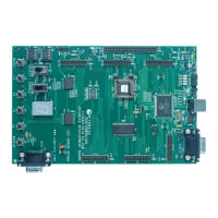
Advanced Development Board
3.3 Jumpers
Table 3-1. EZ-USB Development Board Jumpers
3.4 EEPROM Select and Enable Switches SW1 and SW2
SW1 selects between two socketed EEPROMs, one strapped to address 000 (U6), and the other
strapped to address 001(U5).
SW2 enables or disables the EEPROM selected by SW1.
The EZ-USB chip has various startup modes, which depend on the existence of an EEPROM
connected to its SCL and SDA lines. Switches SW1 and SW2 allow the EEPROMs to be
disconnected from FX1/FX2LP, or to be connected using one of the two EEPROMs installed in
sockets U5 and U6.
The EZ-USB chip contains two I
2
C controllers, a “boot load” controller and an 8051 controller. The
boot load controller operates when EZ-USB comes out of reset, and the 8051 controller operates
under firmware control when the 8051 is running, allowing the 8051 to access general-purpose I
2
C
devices connected to the SCL and SDA lines. The following section deals with the roles of SW1 and
SW2 in accommodating the various boot load mechanisms.
The EZ-USB bootloader accommodates two EEPROM types, in “Small” and “Large” versions, as
shown in Table 3-2.
Jumper Function Default Notes
JP1, JP10
Connects 3.3 V power to
the EZ-USB chip.
IN (1-2)
JP2
Powers the on-board 3.3 V
regulator from USB Vbus
pin
IN (1-2)
To operate the board in self-powered mode, remove
JP2 and supply 4 V to 5 V to JP2-1, and GND to a
ground pin (TP1 is a convenient GND point).
JP3
Connects four GAL pins to
LEDS D2, D3, D4, D5
IN (1-2) (3-4)
(5-6) (7-8)
U2, the on-board GAL, contains code to use the four
LEDs as software indicators that can be set. To use
the GAL pins for something else, which requires re-
programming the GAL or to wire the general purpose
indicators D2-D5 to other parts of the board, first
remove the appropriate shorting plug(s).
JP5 3.3 V power IN (1-2)
Supplies 3.3-V power to the board. It can be removed
and replaced with ammeter probes in series to mea-
sure board current.
JP6, JP7 Memory map selection OUT (1-2)
These jumpers select one of the four memory maps
for U3, the external 128 KB RAM. See Memory Maps
on page 26 for details.
JP8 Wakeup2 pin OUT (1-2)
Inserting a shorting plug into JP8 connects an on-
board RC network (R42,C43) to the secondary
remote wakeup pin WU2. This R-C network can be
used to test the periodic remote wakeup firmware
when this dual-purpose pin (it defaults to PA3) is pro-
grammed as WU2.
JP9
I
2
C bus test points
N/A
The I
2
C bus SCL and SDA lines can be monitored or
externally connected using JP9.