EZ-USB Development Kit User Guide, Doc. # 001-66390 Rev. *D 25
Advanced Development Board
3.6 ATA Connector P8
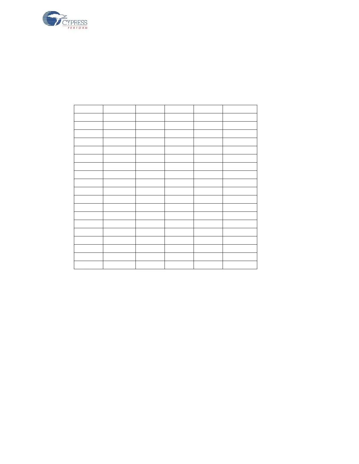
Table 3-10 shows the pinout for P8, a 40-pin connector that interfaces with a standard ATA cable.
This is for ATA use only. SP1, 2, and 3 should be bridged with the solder to connect the appropriate
pull-up and pull-down resistors required for ATA. An 80-pin cable is required for UDMA transfer
modes and recommended for all transfer modes.
Table 3-10. P8 (ATA)
3.7 U2 - 22v10 Gate Array Logic (GAL)
A standard 22v10 GAL provides a general-purpose “glue logic” on the board. It provides the AND
gate required to combine the PSEN and READ signals, adds memory map support, debug LEDs,
and provides three spare outputs for customer-defined functions.
RESET# PA7 1 2 GND GND
DD7 PB7 3 4 PD0 DD8
DD6 PB6 5 6 PD1 DD9
DD5 PB5 7 8 PD2 DD10
DD4 PB4 9 10 PD3 DD11
DD3 PB3 11 12 PD4 DD12
DD2 PB2 13 14 PD5 DD13
DD1 PB1 15 16 PD6 DD14
DD0 PB0 17 18 PD7 DD15
GND GND 19 20 N.C. KEYPIN
DMARQ RDY1 21 22 GND GND
DIOW# CTL0 23 24 GND GND
DIOR# CTL1 25 26 GND GND
IORDY RDY0 27 28 GND CSEL
DMACK# CTL2 29 30 GND GND
INTRQ PA0 31 32 N.C. RESERVED
DA1 PA2 33 34 N.C. PDIAG#
DA0 PA1 35 36 PA3 DA2
CS0#PA43738PA5CS1#
DASP# 10K Pull-up 39 40 GND GND