EZ-USB Development Kit User Guide, Doc. # 001-66390 Rev. *D 91
EZ-USB Development Kit Firmware Examples
//Clear Flags
EXIF &= 0xBF; // Clear INT4 EXIF.6 Flag
EXIF &= 0x7F; // Clear INT5 EXIF.7 Flag
EICON &= 0xF7; // Clear INT6 EICON.3 Flag
EA = 1; // Enable Global Interrupt
The Interrupt service routines for each of these external interrupts are defined in "isr.c". These rou-
tines clear the interrupt and toggle the relevant port pin and any one of the LEDs from D2 to D5.
void ISR_EXTR4(void) interrupt 10
{
EXIF &= 0xBF; // Clear INT4 EXIF.6 Flag
IOC ^= 0x10; // Toggle pin 4 of PortC
}
The example is compiled using the Keil IDE similar to previous examples and corresponding images
for RAM (extr_intr.hex) and EEPROM (extr_intr.iic) can be generated. Both the images are located
at <Installed_directory>\<version\extr_intr. Download the images using the process
outlined in Method to Download Firmware Image to EZ-USB Internal RAM Memory on page 69 and
Method to Download Firmware Image to External I2C EEPROM on page 69.
8.12.1 Testing the Example
The function generator can be set to generate a square wave of a known frequency (use a low fre-
quency - for example, a 100-Hz signal to view LED toggling). When the respective interrupts are trig-
gered, the LED toggle appears. When an INT0 interrupt occurs, PC.0 and D2 are toggled. Similarly,
on INT1/ INT4/ INT5/ INT6, PC.1 and D3/ PC.4 and D4/ PC.5 and D5/ PC.6 are toggled. Port C pin
toggling can be checked by connecting those pins to the DSO.
8.13 Vend_ax Example
This example demonstrates the use of different vendor commands. Vendor commands are used to
accomplish unique tasks, such as EZ-USB reset, RAM download, setting different frequency for the
I2C interface of EZ-USB, communicate with an external SRAM memory, and so on. The vendor
commands are defined in the vend_ax.c source file of the example. Open the project by clicking on
vend_ax.uv2.
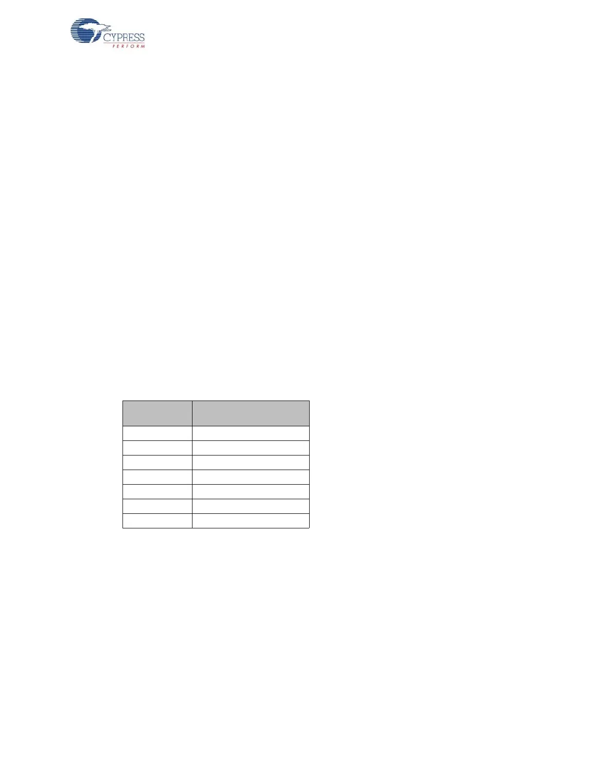
Table 8-4. Port Pins and External Interrupt Mapping
Pin Name
Port/Jumper name on
CY3684/CY3674
Port C P3
LEDs JP3
INT0 P2.19
INT1 P2.18
INT4 P6.5
INT5 P6.4
INT6 PE.5