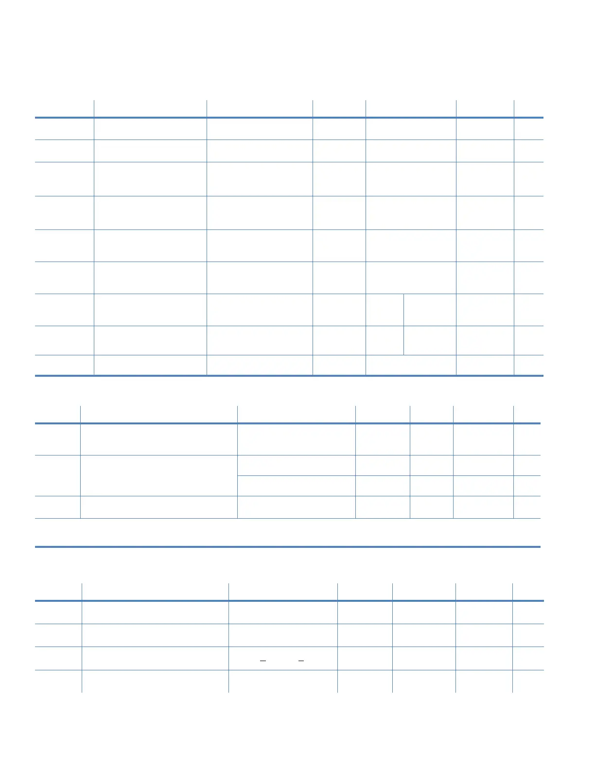
Electrical characteristics of the XBee/XBee-PRO RF Module
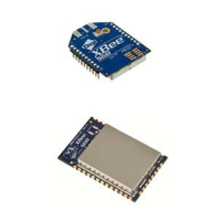
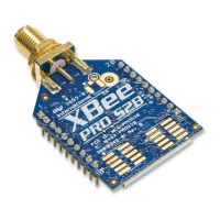
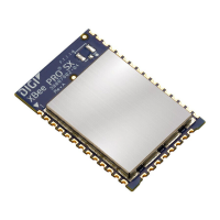
XBee / XBee-PRO RF Modules 802.15.4 Product Manual 16
Electrical characteristics of the XBee/XBee-PRO RF Module
Table 3: DC Characteristics (VCC = 2.8 - 3.4 VDC)
Symbol Characteristic Condition Min Typical Max Unit
V
IL
Input Low Voltage All Digital Inputs
--
0.35 * VCC
V
V
IH
Input High Voltage All Digital Inputs 0.7 * VCC
--V
V
OL
Output Low Voltage I
OL
= 2 mA, VCC >= 2.7
V
--0.5V
V
OH
Output High Voltage I
OH
= -2 mA, VCC >=
2.7 V
VCC - 0.5
--V
II
IN
Input Leakage Current VIN = VCC or GND, all
inputs, per pin
-0.0251μA
II
OZ
High Impedance
Leakage Current
VIN = VCC or GND, all
I/O High-Z, per pin
-0.0251μA
TX Transmit current VCC = 3.3 V
-
45
(XBee)
215, 140
(PRO, Intl)
-mA
RX Receive Current VCC = 3.3 V
-
50
(XBee)
55 (PRO) - mA
PWR-DWN Power-down Current SM parameter = 1
-< 10 -μA
Table 4: ADC characteristics (operating)
Symbol Characteristic Condition Min Typical Max Unit
V
REFH
VREF - analog-to-digital converter
reference range
2.08 - V
DDAD*
V
I
REF
VREF - reference supply current Enabled - 200 - μA
Disabled or Sleep Mode - < 0.01 0.02 μA
V
INDC
Analog input voltage** V
SSAD
- 0.3 - V
DDAD
+ 0.3 V
* V
DDAD
is connected to VCC.
** Maximum electrical operating range, not valid conversion range.
Table 5: ADC timing/performance characteristics
1
Symbol Characteristic Condition Min Typical Max Unit
R
AS
Source impedance at input
2
-- 10k
V
AIN
Analog input voltage
3
V
REFL
V
REFH
V
RES
Ideal resolution (1 LSB)
4
2.08V < V
DDAD
< 3.6V 2.031 - 3.516 mV
DNL
Differential non-linearity
5
- ±0.5 ±1.0 LSB