5 CAMERA FUNCTIONAL DESCRIPTION
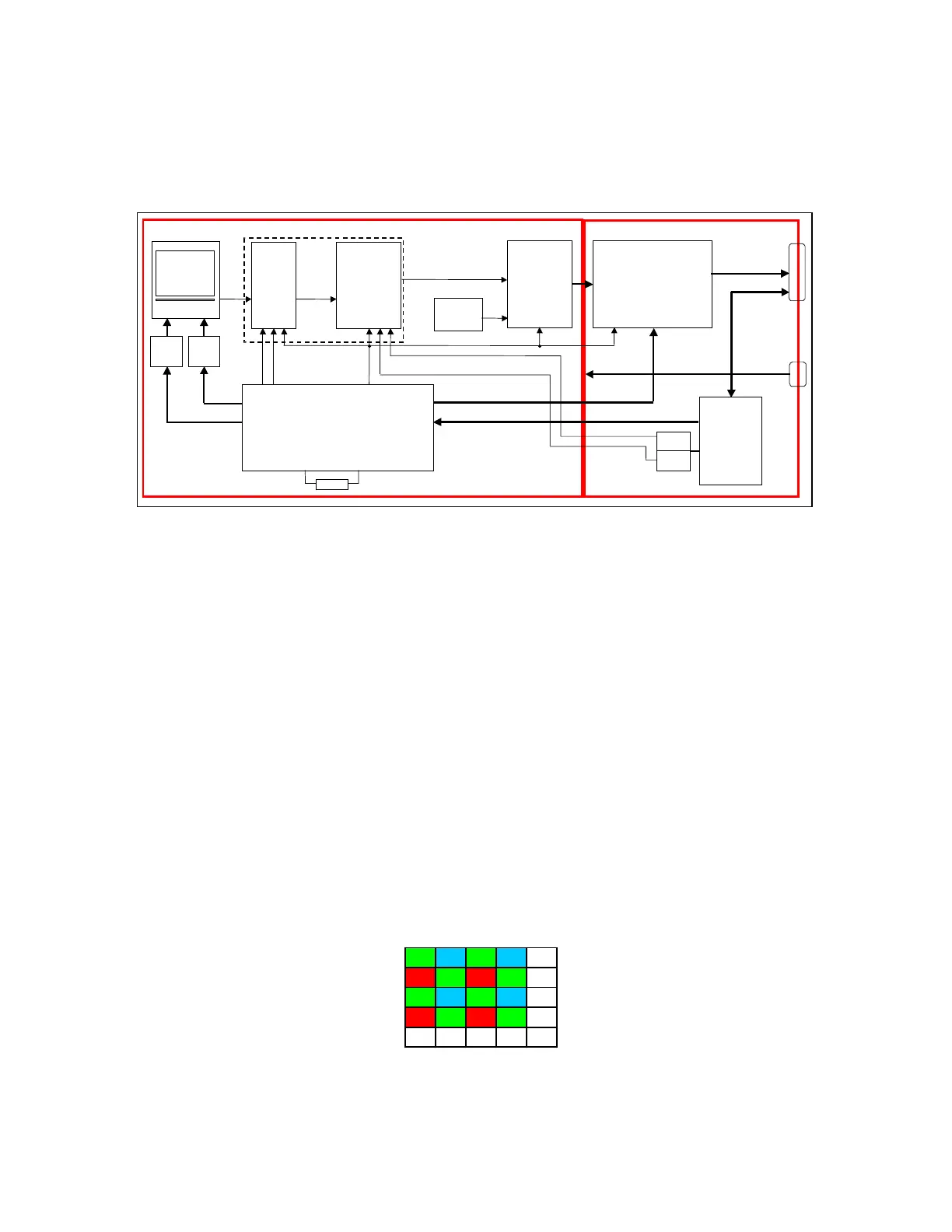
5.1 BLOCK DIAGRAM
S/H CCD
Video
CCD Sensor
CDS
(Correlated
Double
Sampling)
Video amplifier:
Gain control
Offset control
Clamping
A/D reference
generation
A/D Converter
Analog/Digital
conversion
TTL to LVDS drivers:
single ended TTL to parallel,
differential LVDS output
Imaging
Area
(1300 x 1030)
Timing logic:
Clock generation
Generation of all CCD control signals
Generation of all handshaking signals
Exposure control
CCD and Video Board
Processed CCD Video
CCD
Video
Horizontal
Vertical
S/H signals
Timing signals
DB9-M Connector
(Pwr Supply)
+15V,-15V,+5V
DB-44 F
connector
(Digital
Video)
Horiz.
Driver
Vertical
Drivers
I/O board
Microprocessor:
RS232 interface
Mode logic
Gain/offset control
Gain
DAC
Offset
DAC
Mode/Exposure control
Gain control
voltage (0 to 3V)
Offset control
voltage (0 to 3V)
Crystal
Handshaking signals
RS232
signals
A/D
references
Camera
Figure 5.1-1: DVC-1412 camera block diagram (LVDS version shown)
5.2 CCD AND VIDEO BOARD
5.2.1 CCD Sensor
Light from the scene is brought into focus at the imaging plane of the CCD. A 1mm thick infrared
blocking optical removable filter blocks out the IR component of the light. The IR blocking filter is
attached to the c-mount adapter ring. For non IR multi-spectral imaging applications with the
DVC-1412 AC Mount Adapter without an IR filter is available.
The following functions take place within the CCD:
5.2.1.1 Integration
During the integration period (1/10 sec.), charges are integrated in the active charge site wells. The
amount of charge that is integrated in each active charge site well is proportional to the
illumination received at each active charge site on the CCD. In the case of the color camera, each
charge site has a Red, Green or Blue color filter over the field, designating it as a Red, Green or
Blue pixel. The filter pattern that is used is referred to as a Bayer pattern, which is shown below:
GBGB ..
RGRG..
GBGB ..
RGRG..
::::::
Figure 5.2-1: Bayer pattern color filter array
13