EasyManua.ls Logo

Epson RX4111CE - Chargeable Current Characteristics; Reference Value of Switching Element; Table 6 Reference Value of Switching Element

Epson RX4111CE
61 pages
Print Icon
To Next Page IconTo Next Page
To Previous Page IconTo Previous Page
Loading...
RX4111CE Jump to Top / Bottom
ETM62E-02 Seiko Epson Corporation 11
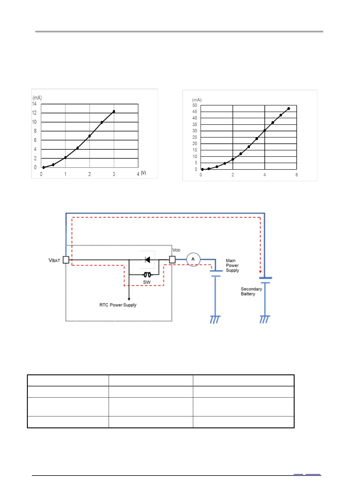
9.1.2. Chargeable Current Characteristics







Figure 10 Chargeable current of VBAT (VDD = 3.0 V)
Figure 11 Chargeable Current of VBAT (VDD = 5.5V)
Figure 12 Circuit of charge to Re-chargeable Battery
9.1.3. Reference Value of Switching Element
Table 6 Reference value of switching element
Item
Characteristics
Condition
Current tolerance
40 mA Max.
SW = ON +25 °C
Diode Vf
0.60 V / 1 mA Typ.
0.85 V / 10 mA Typ.
V
DD
= 3.0 V, +25 °C
Diode IR
5 nA (Max.)
VR = 5.5 V, -40 °C +85 °C
Charge current into V
BAT
should be less than 40 mA.
V
DD
= 3.0 V Vdif (V) vs Ichg (mA)
V
DD
= 5.5 V Vdif (V) vs Ichg (mA)
(V)

Table of Contents

Related product manuals