10. Interface timing when power ON / OFF
RX4111CE Jump to Top / Bottom
ETM62E-02 Seiko Epson Corporation 13
9.2.2. AC Characteristics
Table 8 FOUT symmetry
Unless otherwise specified、GND=0 V , V
IO
= 1.6 V 5.5 V , Ta= -40 C +85 C
10.1. Restrictions of SPI-Bus interface in the power ON / OFF.
t
R1
is needed for a proper power-on reset. If this power-on condition cannot be kept, it is necessary to reset the device by means
of a software command.
After all power-OFF, keep VDD = VBAT = GND for more than 10 seconds for a proper power-on reset by cold start.
When cannot it, please initialize the RTC by software.
The backup period against this standard does not indicate the noise characteristics with respect to the power supply.
The backup period should be long enough (60 seconds or more).
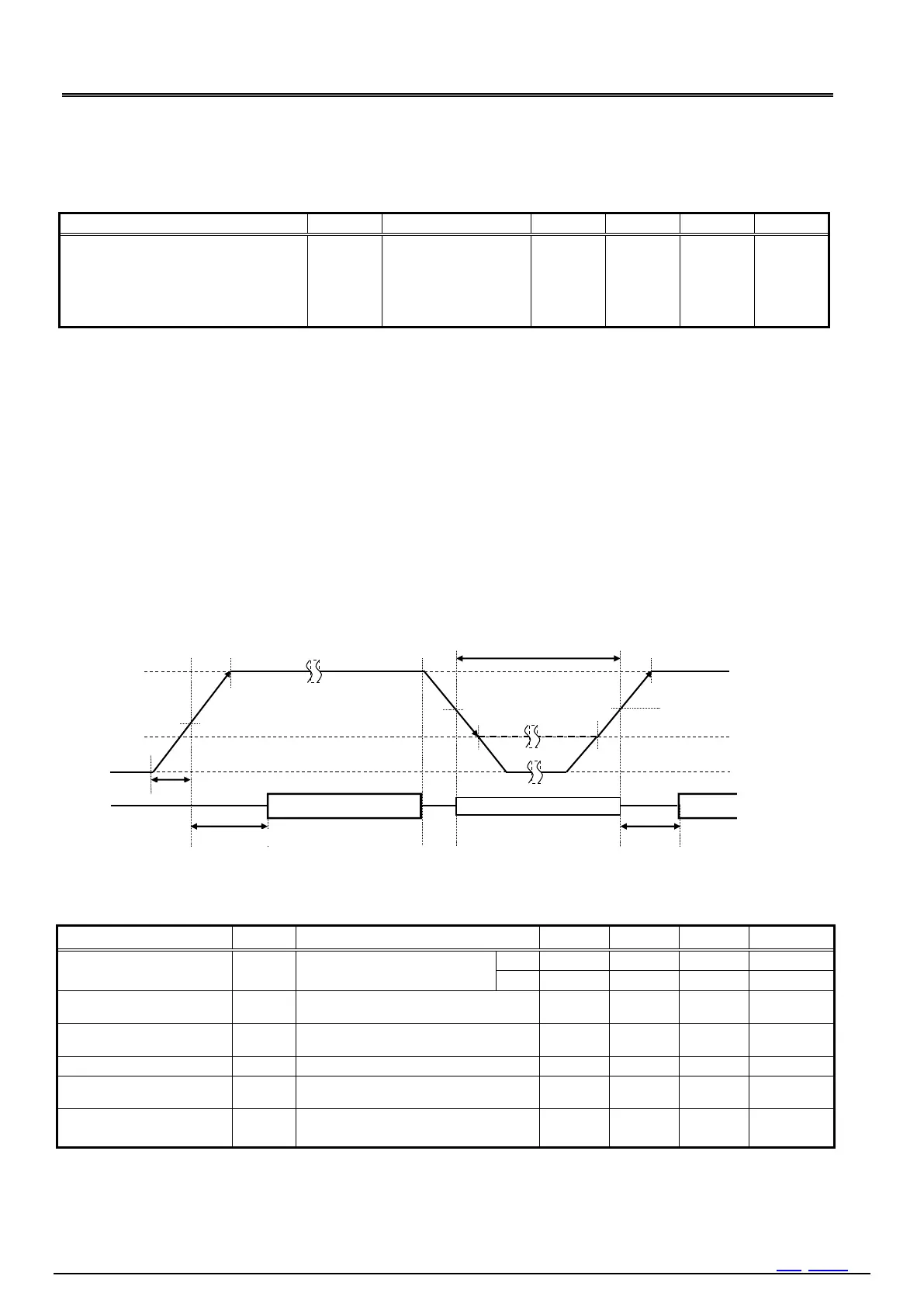
Figure 14 Power on Sequence
Table 9 Power up down characteristics
Initial power supply rise
time
Access wait time
(Initial power on)
After arrival to V
DD
= 1.6 V
Backup switchover start
wait time
Power supply rise time
(Recovery from Backup)
Recovery to the operating voltage
Access wait time
(Recovery from Backup)
The time from Recovery from
Backup to access start
1 Power-on reset is performed at the rising edge of V
BAT
or V
DD
.
2 Since the V
DD
voltage monitoring (+V
DET1
) during backup is intermittent operation (31.25 ms) , a delay occurs after V
DD
reaches
+V
DET1
until the power supply switches.
*3 For internal initialization, the V
DD
voltage at the initial power-on must be increased to 1.6 V or more.