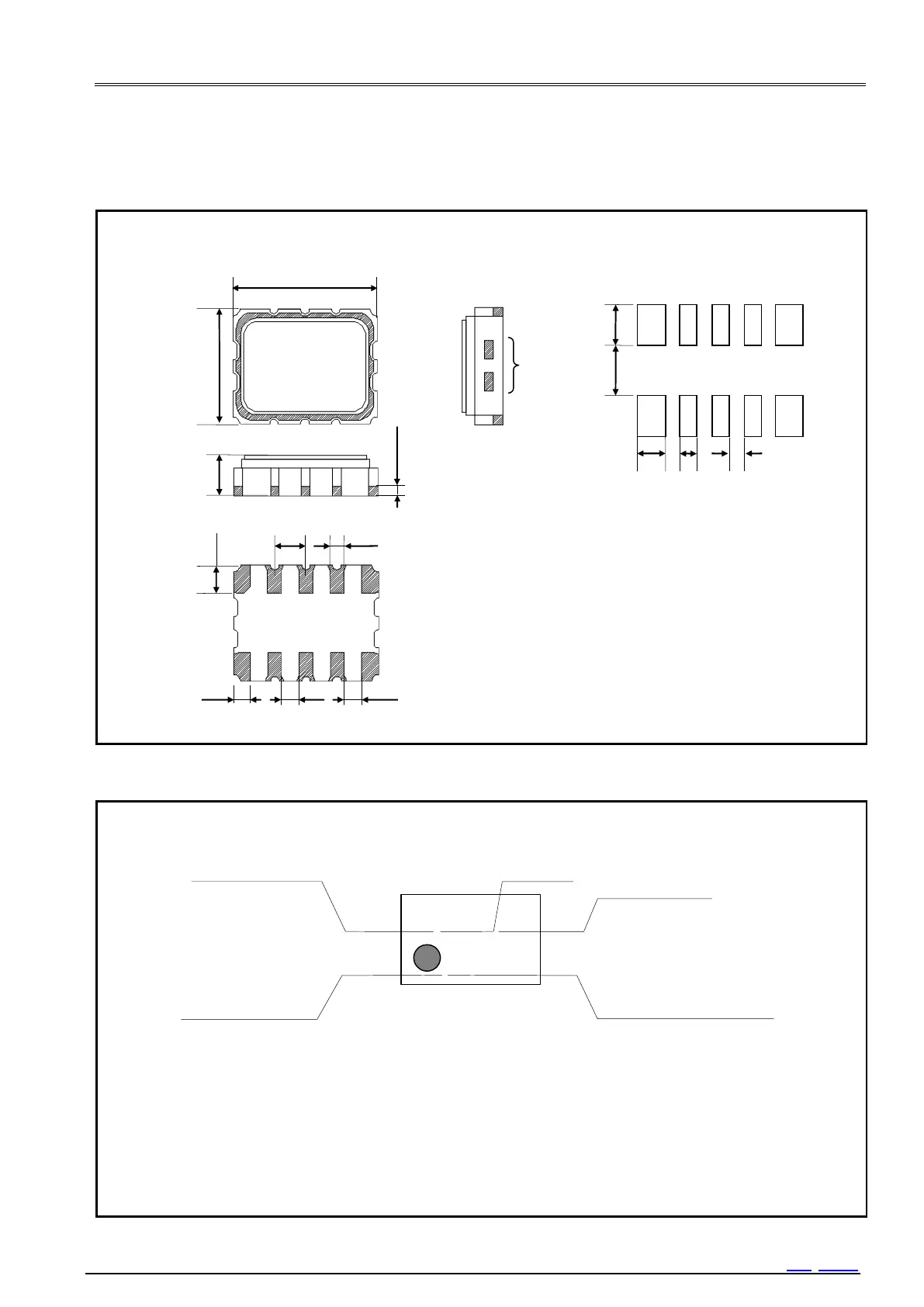
5. External Dimensions / Marking Layout
RX4111CE Jump to Top / Bottom
ETM62E-02 Seiko Epson Corporation 8
5.1. External Dimensions
External Dimensions Recommended soldering pattern
*1. The metal pads on the short side of the 1st and 10th pins of the
package are inspection pads for the crystal unit.
For stable oscillation, make sure that leakage current due to
condensation or dust does not occur between these pads.
The metal pads on the short side of the 5-pin and 6-pin sides are not
connected inside the RTC.
Figure 8 External dimensions
5.2. Marking Layout
Contents displayed indicate the general markings and display, but are not the standards for the fonts, sizes and
positioning.