EasyManua.ls Logo

Epson RX4111CE - Reading;Writing Data Via the SPI-Bus Interface; Write; Read and Bank Select; Write of Data; Read of Data

Epson RX4111CE
61 pages
Print Icon
To Next Page IconTo Next Page
To Previous Page IconTo Previous Page
Loading...
14. How to use
RX4111CE Jump to Top / Bottom
ETM62E-02 Seiko Epson Corporation 56
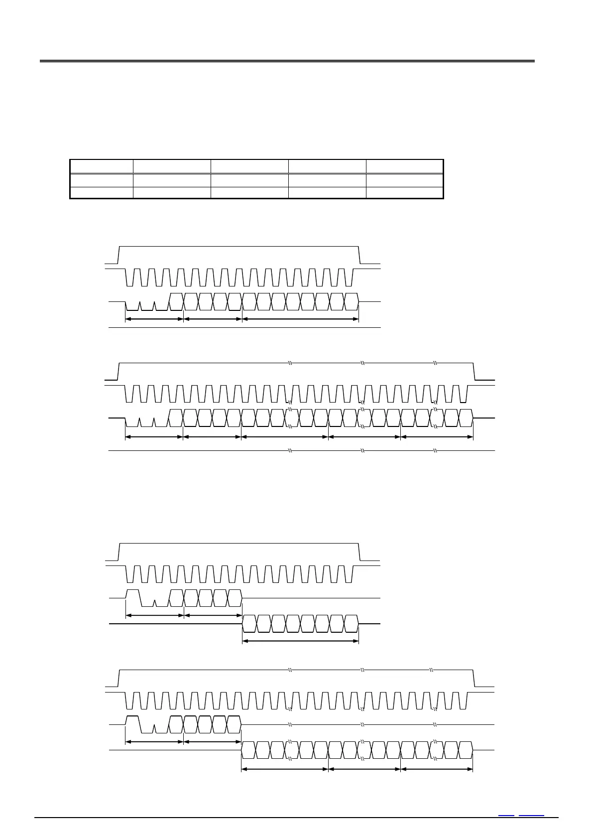
14.10. Reading/Writing Data via the SPI-Bus Interface
For both read and write, first set up chip condition (internally CE="H") to CE="H", then specify the 4-bits address, and
finally read or write in 8-bits units. Both read and write use MSB-first. In continuous operation, objected address is auto
incremented. Auto incrementing of the address is cyclic, so address "F" is followed by address 0.
14.10.1 Write / Read and Bank Select
R/W and Register bank are specified by the four bits mode setting code.
Mode
Bank1
Bank2
Bank3
Bank6
Read
9h
Ah
Bh
Eh
Write
1h
2h
3h
6h
Bank5 and Bank6 are for software reset
14.10.2 Write of Data
1) One-shot writing
CLK
C E
D I
D O
Hi-Z
0
0
0
1
A3
A2
A1
A0
D7
D6
D5
D4
D3
D2
D1
D0
1 2 3 4 5 6 7 8 9 10 11 12 13 14 15 16
Mode
Address N
Data N
2 ) Continuous writing
CLK
C E
D I
D O
Hi-Z
0
0
1
A3
A2
A1
A0
D7
D6
D5
D1
D0
D7
D6
1 2 3 4 5 6 7 8 9 10 11
D1
D0
D7
D6
D1
D0
0
Mode
Address N
Data N
Data N+1
Data N+m
When writing data, the data needs to be entered in 8-bits units.
If the input of data in 8-bits unit is not completed before CE input falls, the 8-bits data will not be written properly
at the time CE input falls.
14.10.3 Read of Data
1) One-shot reading
CLK
C E
D I
D O
Hi-Z
1
0
0
1
A3
A2
A1
A0
D7
D6
D5
D4
D3
D2
D1
D0
1 2 3 4 5 6 7 8 9 10 11 12 13 14 15 16
Mode
Address N
Data N
2 ) Continuous reading
CLK
C E
D I
D O
Hi-Z
1
0
1
A3
A2
A1
A0
D7
D6
D5
D1
D0
D7
D6
1 2 3 4 5 6 7 8 9 10 11
D1
D0
D7
D6
D1
D0
0
Mode
Address N
Data N
Data N+1
Data N+m

Table of Contents

Related product manuals